
“When I look inside a chip from the popular 7400 series, I know what to expect: a fairly simple die, implemented in a straightforward, cost-effective way. However, when I looked inside a military-grade chip built by Integrated Device Technology (IDT)4 I found a very unexpected layout: over 1500 transistors in an orderly matrix. Even stranger, most of the die is wasted: less than 20% of these transistors are used, forming scattered circuits connected by thin metal wires.
In this blog post, I look at this chip in detail, describe its gates, and explain how it implements the “1-of-4” decoder function. I also discuss why it sometimes makes sense to build chips with a gate array design such as this, despite the inefficiency.
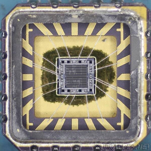
In the photo below, you can see the silicon die in more detail, with the silicon appearing pink. The main circuitry is implemented in the nine rows that form the gate array, a grid of 1584 transistors. The tiny dark rectangles are transistors of two types, NMOS and PMOS, that work together to implement CMOS logic circuits. At this scale, the metal wiring is visible as faint gray lines and smudges, but most of the transistors are unconnected. Surrounding the gate array are 22 input/output (I/O) blocks each with a square bond pad. As with the transistors, many of these I/O blocks are unused. Fourteen of these bond pads have tiny metal bond wires (the thick black lines) that connect the silicon die to the chip’s external pins. Finally, the pairs of bond wires at the center left and center right provide ground and power connections for the chip.”