
“You might think of the Intel 386 processor (1985) as just an early processor in the x86 line, but the 386 was a critical turning point for modern computing in several ways.1 First, the 386 moved the x86 architecture to 32 bits, defining the dominant computing architecture for the rest of the 20th century. The 386 also established the overwhelming importance of x86, not just for Intel, but for the entire computer industry. Finally, the 386 ended IBM’s control over the PC market, turning Compaq into the architectural leader.
In this blog post, I look at die photos of the Intel 386 processor and explain what they reveal about the history of the processor, such as the move from the 1.5 µm process to the 1 µm process. You might expect that Intel simply made the same 386 chip at a smaller scale, but there were substantial changes to the chip’s layout, even some visible to the naked eye. I also look at why the 386 SL had over three times the transistors as the other 386 versions.
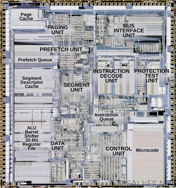
The 80386 was a major advancement over the 286: it implemented a 32-bit architecture, added more instructions, and supported 4-gigabyte segments. The 386 is a complicated processor (by 1980s standards), with 285,000 transistors, ten times the number of the original 8086.4 The 386 has eight logical units that are pipelined and operate mostly autonomously. The diagram below shows the internal structure of the 386.
The heart of a processor is the datapath, the components that hold and process data. In the 386, these components are in the lower left: the ALU (Arithmetic/Logic Unit), a barrel shifter to shift data, and the registers. These components form regular rectangular blocks, 32 bits wide. The datapath, along with the circuitry to the left that manages it, forms the Data Unit. In the lower right is the microcode ROM, which breaks down machine instructions into micro-instructions, the low-level steps of the instruction. The microcode ROM, along with the microcode engine circuitry, forms the Control Unit.
The 386 has a complicated instruction format. The Instruction Decode Unit breaks apart an instruction into its component parts and generates a pointer to the microcode that implements the instruction. The instruction queue holds three decoded instructions. To improve performance, the Prefetch Unit reads instructions from memory before they are needed, and stores them in the 16-byte prefetch queue.
The 386 implements segmented memory and virtual memory, with access protection.9 The Memory Management Unit consists of the Segment Unit and the Paging Unit: the Segment Unit translates a logical address to a linear address, while the Paging Unit translates the linear address to a physical address. The segment descriptor cache and page cache (TLB) hold data about segments and pages; the 386 has no on-chip instruction or data cache.10 The Bus Interface Unit in the upper right handles communication between the 386 and the external memory and devices.
Silicon dies are often labeled with the initials of the designers. The 386 DX, however, has an unusually large number of initials. In the image below, I have enlarged the tiny initials so they are visible. I think the designers put their initials next to the unit they worked on, but I haven’t been able to identify most of the names.”