
“Processors are driven by a clock, which controls the timing of each step inside the chip. In this blog post, I’ll examine the clock-generation circuitry inside the Intel 386 processor. Earlier processors such as the 8086 (1978) were simpler, using two clock phases internally. The Intel 386 processor (1985) was a pivotal development for Intel as it moved x86 to CMOS (as well as being the first 32-bit x86 processor). The 386’s CMOS circuitry required four clock signals. An external crystal oscillator provided the 386 with a single clock signal and the 386’s internal circuitry generated four carefully-timed internal clock signals from the external clock.
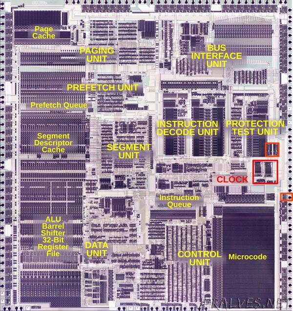
The die photo below shows the Intel 386 processor with the clock generation circuitry and clock pad highlighted in red. The heart of a processor is the datapath, the components that hold and process data. In the 386, these components are in the lower left: the ALU (Arithmetic/Logic Unit), a barrel shifter to shift data, and the registers. These components form regular rectangular blocks, 32 bits wide. In the lower right is the microcode ROM, which breaks down machine instructions into micro-instructions, the low-level steps of the instruction. Other parts of the chip prefetch and decode instructions, and handle memory paging and segmentation. All these parts of the chip run under the control of the clock signals.
A brief discussion of clock phases
Many processors use a two-phase clock to control the timing of the internal processing steps. The idea is that the two clock phases alternate: first phase 1 is high, and then phase 2 is high, as shown below. During each clock phase, logic circuitry processes data. A circuit called a “transparent latch” is used to hold data between steps.2 The concept of a latch is that when a latch’s clock input is high, the input passes through the latch. But when the latch’s clock input is low, the latch remembers its previous value. With two clock phases, alternating latches are active one at a time, so data passes through the circuit step by step, under the control of the clock.
The two-phase clock signal used by the Intel 8080 processor. The 8080 uses asymmetrical clock signals, with phase 2 longer than phase 1. From the 8080 datasheet.
The two-phase clock signal used by the Intel 8080 processor. The 8080 uses asymmetrical clock signals, with phase 2 longer than phase 1. From the 8080 datasheet.
The diagram below shows an abstracted model of the processor circuitry. The combinational logic (i.e. the gate logic) is divided into two blocks, with latches between each block. During clock phase 1, the first block of latches passes its input through to the output. Thus, values pass through the first logic block, the first block of latches, and the second logic block, and then wait.”