
“The 386 processor (1985) was Intel’s most complex processor at the time, with 285,000 transistors. Intel had scheduled 50 person-years to design the processor, but it was falling behind schedule. The design team decided to automate chunks of the layout, developing “automatic place and route” software.1 This was a risky decision since if the software couldn’t create a dense enough layout, the chip couldn’t be manufactured. But in the end, the 386 finished ahead of schedule, an almost unheard-of accomplishment.
In this article, I take a close look at the “standard cells” used in the 386, the logic blocks that were arranged and wired by software. Reverse-engineering these circuits shows how standard cells implement logic gates, latches, and other components with CMOS transistors. Modern integrated circuits still use standard cells, much smaller now, of course, but built from the same principles.
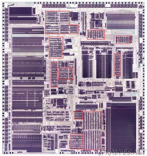
The photo below shows the 386 die with the automatic-place-and-route regions highlighted in red. These blocks of unstructured logic have cells arranged in rows, giving them a characteristic striped appearance. In comparison, functional blocks such as the datapath on the left and the microcode ROM in the lower right were designed manually to optimize density and performance, giving them a more solid appearance. As for other features on the chip, the black circles around the border are bond wire connections that go to the chip’s external pins. The chip has two metal layers, a small number by modern standards, but a jump from the single metal layer of earlier processors such as the 286. The metal appears white in larger areas, but purplish where circuitry underneath roughens its surface. For the most part, the underlying silicon and the polysilicon wiring on top are obscured by the metal layers.
Early processors in the 1970s were usually designed by manually laying out every transistor individually, fitting transistors together like puzzle pieces to optimize their layout. While this was tedious, it resulted in a highly dense layout. Federico Faggin, designer of the popular Z80 processor, describes finding that the last few transistors wouldn’t fit, so he had to erase three weeks of work and start over. The closeup of the resulting Z80 layout below shows that each transistor has a different, complex shape, optimized to pack the transistors as tightly as possible.”