
“A key component of any processor is instruction decoding: analyzing a numeric opcode and figuring out what actions need to be taken. The Intel 8086 processor (1978) has a complex instruction set, making instruction decoding a challenge. The first step in decoding an 8086 instruction is something called the Group Decode ROM, which categorizes instructions into about 35 types that control how the instruction is decoded and executed. For instance, the Group Decode ROM determines if an instruction is executed in hardware or in microcode. It also indicates how the instruction is structured: if the instruction has a bit specifying a byte or word operation, if the instruction has a byte that specifies the addressing mode, and so forth.
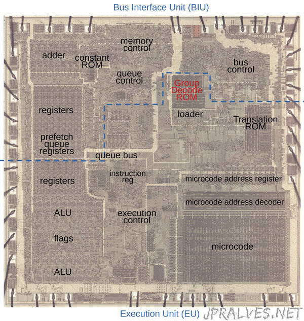
The diagram above shows the position of the Group Decode ROM on the silicon die, as well as other key functional blocks. The 8086 chip is partitioned into a Bus Interface Unit that communicates with external components such as memory, and the Execution Unit that executes instructions. Machine instructions are fetched from memory by the Bus Interface Unit and stored in the prefetch queue registers, which hold 6 bytes of instructions. To execute an instruction, the queue bus transfers an instruction byte from the prefetch queue to the instruction register, under control of a state machine called the Loader. Next, the Group Decode ROM categorizes the instruction according to its structure. In most cases, the machine instruction is implemented in low-level microcode. The instruction byte is transferred to the Microcode Address Register, where the Microcode Address Decoder selects the appropriate microcode routine that implements the instruction. The microcode provides the micro-instructions that control the Arithmetic/Logic Unit (ALU), registers, and other components to execute the instruction.
In this blog post, I will focus on a small part of this process: how the Group Decode ROM decodes instructions. Be warned that this post gets down into the weeds, so you might want to start with one of my higher-level posts, such as how the 8086’s microcode engine works.
Microcode
Most instructions in the 8086 are implemented in microcode. Most people think of machine instructions as the basic steps that a computer performs. However, many processors have another layer of software underneath: microcode. With microcode, instead of building the CPU’s control circuitry from complex logic gates, the control logic is largely replaced with code. To execute a machine instruction, the computer internally executes several simpler micro-instructions, specified by the microcode.
Microcode is only used if the Group Decode ROM indicates that the instruction is implemented in microcode. In that case, the microcode address register is loaded with the instruction and the address decoder selects the appropriate microcode routine. However, there’s a complication. If the second byte of the instruction is a Mod R/M byte, the Group Decode ROM indicates this and causes a memory addressing micro-subroutine to be called.
Some simple instructions are implemented entirely in hardware and don’t use microcode. These are known as 1-byte logic instructions (1BL) and are also indicated by the Group Decode ROM.
The Group Decode ROM’s structure
The Group Decode ROM takes an 8-bit instruction as input, along with an interrupt signal. It produces 15 outputs that control how the instruction is handled. In this section I’ll discuss the physical implementation of the Group Decode ROM; the various outputs are discussed in a later section.
Although the Group Decode ROM is called a ROM, its implementation is really a PLA (Programmable Logic Array), two levels of highly-structured logic gates.1 The idea of a PLA is to create two levels of NOR gates, each in a grid. This structure has the advantages that it implements the logic densely and is easy to modify. Although physically two levels of NOR gates, a PLA can be thought of as an AND layer followed by an OR layer. The AND layer matches particular bit patterns and then the OR layer combines multiple values from the first layer to produce arbitrary outputs.”