
“The 8086 microprocessor was a groundbreaking processor introduced by Intel in 1978. It led to the x86 architecture that still dominates desktop and server computing. While reverse-engineering the 8086 from die photos, a particular circuit caught my eye because its physical layout on the die didn’t match the surrounding circuitry. This circuit turns out to implement special functionality for a couple of instructions, subtlely changing the way they interacted with interrupts. Some web searching revealed that this behavior was changed by Intel in 1978 to fix a problem with early versions of the 8086 chip. By studying the die, we can get an idea of how Intel dealt with bugs in the 8086 microprocessor.
In modern CPUs, bugs can often be fixed through a microcode patch that updates the CPU during boot.1 However, prior to the Pentium Pro (1995), microprocessors could only be fixed through a change to the design that fixed the silicon. This became a big problem for Intel with the famous Pentium floating-point division bug. The chip turned out to have a bug that resulted in rare but serious errors when dividing. Intel recalled the defective processors in 1994 and replaced them, at a cost of $475 million.
The circuit on the die
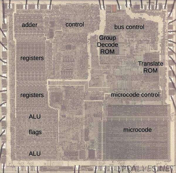
The microscope photo below shows the 8086 die with the main functional blocks labeled. This photo shows the metal layer on top of the silicon. While modern chips can have more than a dozen layers of metal, the 8086 has a single layer. Even so, the metal mostly obscures the underlying silicon. Around the outside of the die, you can see the bond wires that connect pads on the chip to the 40 external pins.
The relevant part of the chip is the Group Decode ROM in the upper center. The purpose of this circuit is to categorize instructions into groups that control how they are decoded and processed. For instance, very simple instructions (such as setting a flag) can be performed directly in one cycle. Other instructions are not complete instructions, but a prefix that modifies the following instruction. The remainder of the instructions are implemented in microcode, which is stored in the lower-right corner of the chip. Many of these instructions have a second byte, the “Mod R/M” byte that specifies a register and the memory addressing scheme. Some instructions have two versions: one for an 8-bit operand and one for a 16-bit operand. Some operations have a bit to swap the source and destination. The Group Decode ROM is responsible for looking at the 8 bits of the instruction and deciding which groups the instruction falls into.”