
“I recently saw an interesting die photo of an unknown chip on Twitter, so I did some analysis of it. Looking at the circuitry inside, the chip appears to be four comparators, probably in the ECL (Emitter Coupled Logic) family. This is a quick blog post to summarize my investigation.
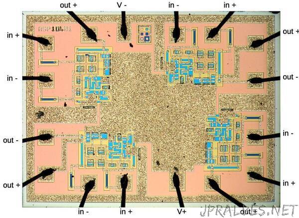
The die photo below shows the chip under the microscope. Regions of the silicon appear pink, blue, or yellow, depending on how the silicon was doped. The speckled regions are the metal layer on top of the silicon, wiring the circuitry together. Around the edges, the black bond wires connect the chip to the external pins. These wires are attached to the square bond pads. The die has four blocks of circuitry, one for each of its four comparators. Much of the die is unused, especially the large metal area in the middle. Because this chip’s circuitry is relatively simple, it only uses a fraction of the available space.
The photo below shows the chip with its metal lid removed. Modern chips are usually in a black epoxy package, but this chip has a white ceramic package. The tiny silicon die is visible in the middle, with bond wires connecting the die to the lead frame, the metal connections to the chip’s gold-plated pins. The metal layer on top of the die is visible, and can be matched with the die photo above. The semi-circular notch on the left indicates the orientation of the chip; the “P” is pin 1.”