
“The Intel 8086 microprocessor (1978) started the x86 architecture that continues to this day. In this blog post, I’m focusing on a small part of the chip: the address and data pins that connect the chip to external memory and I/O devices. In many processors, this circuitry is straightforward, but it is complicated in the 8086 for two reasons. First, Intel decided to package the 8086 as a 40-pin DIP, which didn’t provide enough pins for all the functionality. Instead, the 8086 multiplexes address, data, and status. In other words, a pin can have multiple roles, providing an address bit at one time and a data bit at another time.
The second complication is that the 8086 has a 20-bit address space (due to its infamous segment registers), while the data bus is 16 bits wide. As will be seen, the “extra” four address bits have more impact than you might expect. To summarize, 16 pins, called AD0-AD15, provide 16 bits of address and data. The four remaining address pins (A16-A19) are multiplexed for use as status pins, providing information about what the processor is doing for use by other parts of the system. You might expect that the 8086 would thus have two types of pin circuits, but it turns out that there are four distinct circuits, which I will discuss below.
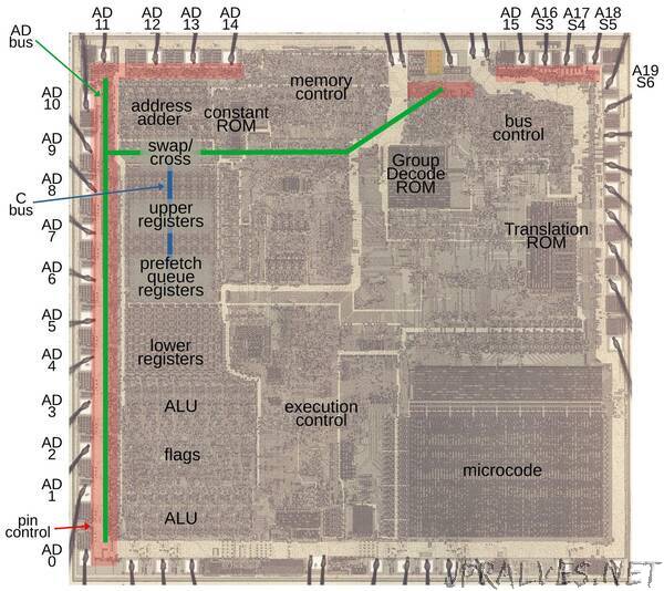
The microscope image above shows the silicon die of the 8086. In this image, the metal layer on top of the chip is visible, while the silicon and polysilicon underneath are obscured. The square pads around the edge of the die are connected by tiny bond wires to the chip’s 40 external pins. The 20 address pins are labeled: Pins AD0 through AD15 function as address and data pins. Pins A16 through A19 function as address pins and status pins.1 The circuitry that controls the pins is highlighted in red. Two internal busses are important for this discussion: the 20-bit AD bus (green) connects the AD pins to the rest of the CPU, while the 16-bit C bus (blue) communicates with the registers. These buses are connected through a circuit that can swap the byte order or shift the value. (The lines on the diagram are simplified; the real wiring twists and turns to fit the layout. Moreover, the C bus (blue) has its bits spread across the width of the register file.)
Segment addressing in the 8086
One goal of the 8086 design was to maintain backward compatibility with the earlier 8080 processor.2 This had a major impact on the 8086’s memory design, resulting in the much-hated segment registers. The 8080 (like most of the 8-bit processors of the early 1970s) had a 16-bit address space, able to access 64K (65,536 bytes) of memory, which was plenty at the time. But due to the exponential growth in memory capacity described by Moore’s Law, it was clear that the 8086 needed to support much more. Intel decided on a 1-megabyte address space, requiring 20 address bits. But Intel wanted to keep the 16-bit memory addresses used by the 8080.
The solution was to break memory into segments. Each segment was 64K long, so a 16-bit offset was sufficient to access memory in a segment. The segments were allocated in a 1-megabyte address space, with the result that you could access a megabyte of memory, but only in 64K chunks.3 Segment addresses were also 16 bits, but were shifted left by 4 bits (multiplied by 16) to support the 20-bit address space.
Thus, every memory access in the 8086 required a computation of the physical address. The diagram below illustrates this process: the logical address consists of the segment base address and the offset within the segment. The 16-bit segment register was shifted 4 bits and added to the 16-bit offset to yield the 20-bit physical memory address.
This address computation was not performed by the regular ALU (Arithmetic/Logic Unit), but by a separate adder that was devoted to address computation. The address adder is visible in the upper-left corner of the die photo. I will discuss the address adder in more detail below.
The AD bus and the C Bus
The 8086 has multiple internal buses to move bits internally, but the relevant ones are the AD bus and the C bus. The AD bus is a 20-bit bus that connects the 20 address/data pins to the internal circuitry.4 A 16-bit bus called the C bus provides the connection between the AD bus, the address adder and some of the registers.5 The diagram below shows the connections. The AD bus can be connected to the 20 address pins through latches. The low 16 pins can also be used for data input, while the upper 4 pins can also be used for status output. The address adder performs the 16-bit addition necessary for segment arithmetic. Its output is shifted left by four bits (i.e. it has four 0 bits appended), producing the 20-bit result. The inputs to the adder are provided by registers, a constant ROM that holds small constants such as +1 or -2, or the C bus.
The shift/crossover circuit provides the interface between these two buses, handling the 20-bit to 16-bit conversion. The busses can be connected in three ways: direct, crossover, or shifted.6 The direct mode connects the 16 bits of the C bus to the lower 16 bits of the address/data pins. This is the standard mode for transferring data between the 8086’s internal circuitry and the data pins. The crossover mode performs the same connection but swaps the bytes. This is typically used for unaligned memory accesses, where the low memory byte corresponds to the high register byte, or vice versa. The shifted mode shifts the 20-bit AD bus value four positions to the right. In this mode, the 16-bit output from the address adder goes to the 16-bit C bus. (The shift is necessary to counteract the 4-bit shift applied to the address adder’s output.) Control circuitry selects the right operation for the shift/crossover circuit at the right time.7
Two of the registers are invisible to the programmer but play an important role in memory accesses. The IND (Indirect) register specifies the memory address; it holds the 16-bit memory offset in a segment. The OPR (Operand) register holds the data value.9 The IND and OPR registers are not accessed directly by the programmer; the microcode for a machine instruction moves the appropriate values to these registers prior to the write.”