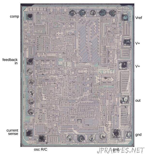
“I recently did a PC power supply teardown so I figured it would be interesting to go deeper and see what happens inside the power supply’s control IC. The die photo below shows the UC3842 chip, which was very popular in older PC power supplies.1 (The chip was introduced in 1984 but this die has a date of 2000.) The tiny silicon die is patterned to create the transistors, resistors and capacitors that make up the circuit. The lighter-colored lines are the metal layer on top of the silicon, forming the chip’s wiring. Around the edges, square pads provide the connections from the die to the IC’s external pins; tiny bond wires connect the pads to the chip’s external pins.”
Related Content
Related Posts:
- Talking to memory: Inside the Intel 8088 processor’s bus interface state machine
- Inside an unusual 7400-series chip implemented with a gate array
- The Intel 8088 processor’s instruction prefetch circuitry: a look inside
- Reverse engineering standard cell logic in the Intel 386 processor
- Inside the Intel 386 processor die: the clock circuit
- Reverse engineering the Intel 386 processor’s register cell
- Examining the silicon dies of the Intel 386 processor
- How flip-flops are implemented in the Intel 8086 processor
- Tracing the roots of the 8086 instruction set to the Datapoint 2200 minicomputer
- A close look at the 8086 processor’s bus hold circuitry