
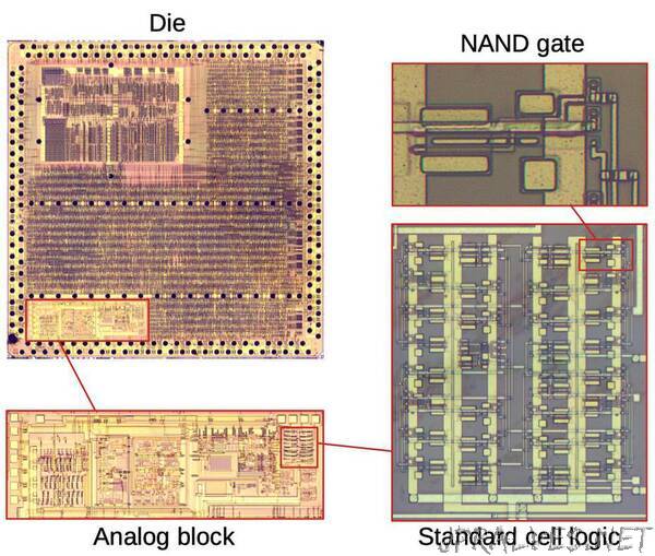
“Integrated circuits are often built from standard-cell logic, constructed from standardized building blocks such as NAND gates. Since I’ve been looking at a chip that uses standard-cell logic, I figured it was a good opportunity to examine standard-cell logic closely by reverse-engineering a simple block of logic on the chip. (It turned out to be a divide-by-16 module.) The diagram below shows the die from an IBM token ring chip from 1993. The chip contains a block of analog network circuitry, but curiously the analog block contains some standard-cell digital logic. Finally, zooming in shows one NAND gate in the logic.
Standard cells let automated tools design a complex integrated circuit from a description in a language such as Verilog. These tools select the appropriate cells from a cell library, place them in rows, and route the wiring between the cells to create the desired logic. This is much easier than a fully-custom design with each individual transistor arranged on the die.1 Vendors supply a library of standard cells2 as well as software to create the design.3 While a library may contain hundreds of different types of cells, the circuit I examined only uses five different cell types, which I will explain below.”