
“In 1969, high-density MOS integrated circuits were still new and logic circuits were constructed in a variety of ways. One technique was “four-phase logic”, which provided ten times the speed and density of standard logic gates while using 1/10 the power.1 One notable application of four-phase logic was calculators. In 1969, Sharp introduced the first calculator built from high-density MOS chips, the QT-8D, followed by the world’s smallest calculator, the handheld EL-8. These calculators were high-end products, selling for $345 (about $1800 today).
Integrated circuits at the time weren’t dense enough to implement an entire calculator on one chip so these calculators split the functionality across five ICs. These five chips were created for Sharp by the Autonetics division of Rockwell. Autonetics invented four-phase logic in the mid-1960s, so this logic family was a natural choice for the calculator chips.
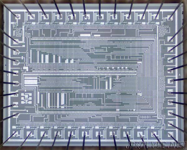
In this blog post, I reverse-engineer the keypad/display chip shown above. This photo shows the tiny silicon die under a microscope. The silicon substrate has a purple tint while the doped, conductive silicon is green. The metal layer on top is white. Around the edges, thin bond wires connect the die to the 42 external pins. The chip contains roughly 500 transistors implementing 100 logic gates. While the density of this chip is absurdly low by modern standards, it illustrates the progress of MOS integrated circuits in the late 1960s.”