
“In 1969, Sharp introduced the first calculator built from high-density MOS chips, the QT-8D, followed by the handheld Sharp EL-8, the world’s smallest calculator at the time.1 These calculators were high-end products, selling for $345 (about $1800 today). Integrated circuits at the time couldn’t fit the entire calculator on one chip, so these calculators contained five ICs: an arithmetic chip, a decimal point chip, a keypad/display chip, a control chip, and a clock chip.
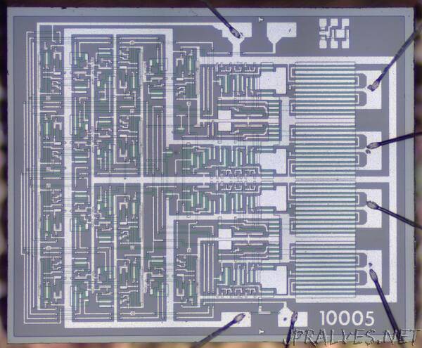
This blog post discusses the clock chip and how it generated the unusual four-phase clock signals required by the calculator. The die photo below, provided by calculator researcher Francois Gueissaz, shows the silicon die of the clock chip. the silicon substrate has a purple tint while the doped, conductive silicon is green. The metal layer on top is white. Around the edges, seven thin bond wires connect the die to the external pins.2 This chip has about 200 transistors and implements just a dozen moderately complex logic gates. While the density of this chip is absurdly low by modern standards, it illustrates the progress of MOS integrated circuits in the late 1960s.
Although computers now all use MOS integrated circuits, the path to MOS was rocky, with MOS integrated circuits viewed as slow and unreliable in the 1960s.4 Handheld calculators were a good match for the characteristics of MOS, though: they needed to be compact and lightweight with low power consumption, but computational speed was not important. In 1969, the Japanese calculator company Sharp signed a $30 million deal with Rockwell for this MOS-based calculator chipset, the largest MOS order in history at the time. The five chips were implemented by the Autonetics division of Rockwell.”