
“The Intel 8086 processor was introduced in 1978, setting the course of modern computing. While the x86 processor family has supported 64-bit processing for decades, the original 8086 was a 16-bit processor. As such, it has a 16-bit arithmetic logic unit (ALU).1 The arithmetic logic unit is the heart of a processor: it performs arithmetic operations such as addition and subtraction. It also carries out Boolean logic operations such as bitwise AND and OR as well as also bit shifts and rotates. Since a fast ALU is essential to the overall performance of a processor, ALUs often incorporate interesting design tricks.
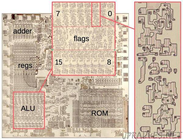
The die photo below shows the silicon die of the 8086 processor. The ALU is in the lower-left corner. Above it are the general- and special-purpose registers. An adder, used for address calculation, is in the upper left. (For performance, the 8086 has a separate adder to add the segment register and memory offset when accessing memory.) The large microcode ROM is in the lower right.
Zooming in on the ALU shows that it is constructed from 16 nearly-identical stages, one for each bit. The upper row handles bits 7 to 0 while the lower row handles bits 15 to 8.3 In between, the flag circuitry indicates the status of an arithmetic operation through condition codes such as zero or nonzero, positive or negative, carry, overflow, parity, and so forth. These are typically used for conditional branches.
In this blog post, I reverse-engineer the 8086’s ALU and explain how it works. It’s more complex than other vintage ALUs that I’ve studied,2 using a flexible circuit that can implement arbitrary bit functions. The carry is implemented with a Manchester carry chain, a fast design dating back to a 1960s supercomputer.”