
“One under-appreciated characteristic of early microprocessors is the difficulty of distributing power inside the integrated circuit. While a modern processor might have 15 layers of metal wiring, chips from the 1970s such as the 8086 had just a single layer of metal, making routing a challenge. Similarly, clock signals must be delivered to all parts of the chip to keep it in synchronization.
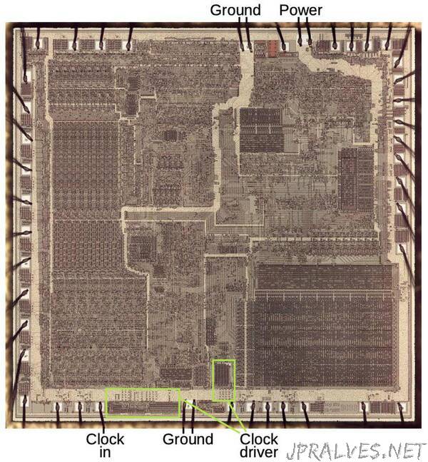
The photo below shows the 8086’s die under a microscope. The metal layer on top of the chip is visible, with the silicon substrate and polysilicon wiring hidden underneath. Around the outside of the die, tiny bond wires connect pads on the die to the external pins. The 8086 has a power pad at the top and ground pads at the top and bottom. Each power and ground pad has two bond wires connected to support twice the current. You can see the wide metal traces from the power and ground pads; these distribute power throughout the chip.
Timing in the 8086 is controlled by two internal clock signals. An external oscillator provides a clock signal to the 8086 through the clock input pad at the bottom. The on-chip clock driver circuitry generates two high-current clock signals from this external clock. Note that the clock driver takes up a not-insignificant part of the chip.
In this blog post, I’ll discuss how the 8086 routes power and clock signals through the chip, and how the clock driver circuit generates the necessary clock pulses.
Power distribution
The 8086 is constructed with three layers that can be used for wiring. The metal layer on top is best for wiring, since metal has low resistance. Underneath the metal is a layer of polysilicon wiring, made from a special type of silicon. Polysilicon has higher resistance than metal, but can still be used to transmit signals across the chip. The silicon substrate is where the transistors are formed. Silicon has relatively high resistance, so it is only used for short-distance connections, such as inside a gate.
Power routing in a chip like the 8086 creates a topological puzzle of sorts: The metal layer is the only practical layer for routing power and ground, due to its low resistance. Power and ground must be provided to nearly every gate in the chip.1 And since the chip has a single metal layer, power and ground can’t cross.
The diagram below highlights these metal wiring networks in the 8086. Power, connected to the power pin at the top, is shown in red, traveling throughout the chip. A major branch flows down and to the right from the power pin, then splitting into multiple paths. Power also travels around the border of the entire chip, supplying the I/O pins.”