Texas Instruments Inc. (TI) is an American technology company that designs and manufactures semiconductors, which it sells to electronics designers and manufacturers globally. Headquartered in Dallas, Texas, United States, TI is one of the top ten semiconductor companies worldwide, based on sales volume. Texas Instruments’s focus is on developing analog chips and embedded processors, which accounts for more than 85% of their revenue.[6] TI also produces TI digital light processing (DLP) technology and education technology products including calculators, microcontrollers and multi-core processors.
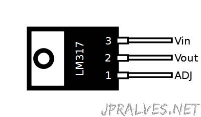
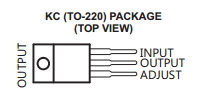
LM317 - 3/4 Pin 1.5A Adjustable Positive Voltage Regulator
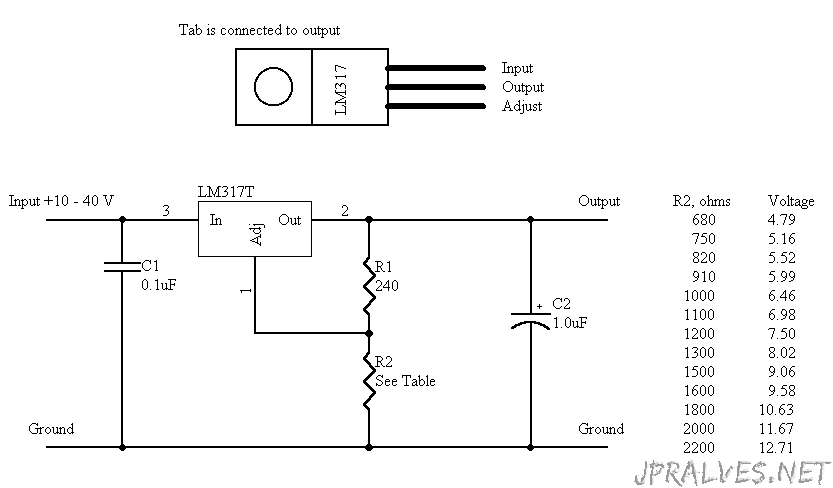
The LM317 is an adjustable three-terminal positive-voltage regulator capable of supplying more than 1.5 A over an output-voltage range of 1.25 V to 37 V. It is exceptionally easy to use and requires only two external resistors to set the output voltage. Furthermore, both line and load regulation are better than standard fixed regulators.
In addition to having higher performance than fixed regulators, this device includes on-chip current limiting, thermal overload protection, and safe operating-area protection. All overload protection remains fully functional, even if the ADJUST terminal is disconnected.
The LM317 is versatile in its applications, including uses in programmable output regulation and local on-card regulation. Or, by connecting a fixed resistor between the ADJUST and OUTPUT terminals, the LM317 can function as a precision current regulator. An optional output capacitor can be added to improve transient response. The ADJUST terminal can be bypassed to achieve very high ripple-rejection ratios, which are difficult to achieve with standard three-terminal regulators.
CSD18504KCS - 40V N-Channel NexFET™ Power MOSFET
The NexFET™ power MOSFET has been designed Continuous Drain Current (Package limited), 100 to minimize losses in power conversion applications.
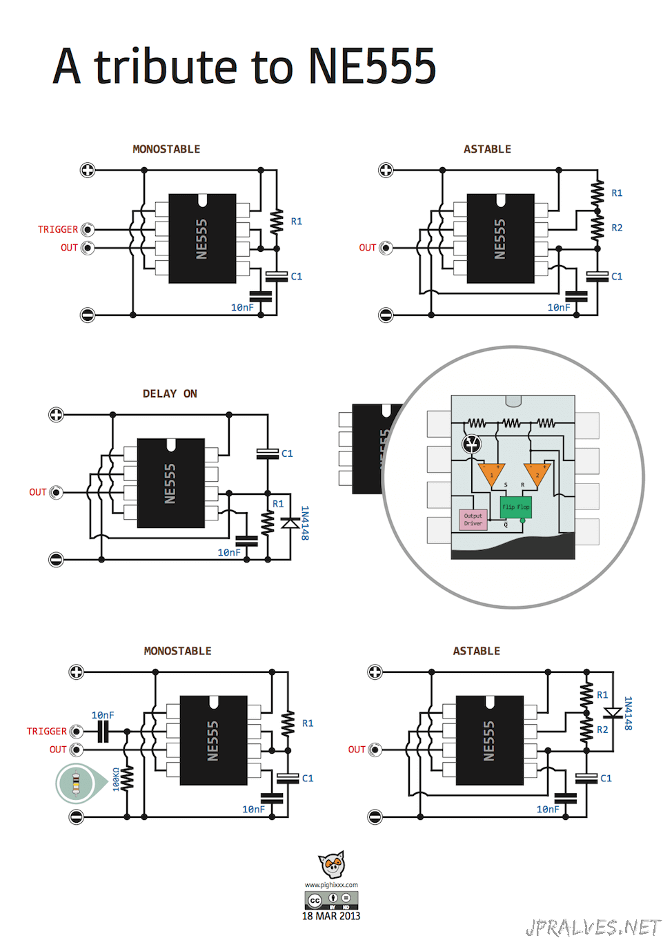
NE555P - Single Precision Timer
The 555 timer IC is an integrated circuit (chip) used in a variety of timer, pulse generation, and oscillator applications. The 555 can be used to provide time delays, as an oscillator, and as a flip-flop element. Derivatives provide up to four timing circuits in one package.
Introduced in 1971 by Signetics, the 555 is still in widespread use due to its ease of use, low price, and stability. It is now made by many companies in the original bipolar and also in low-power CMOS types. As of 2003, it was estimated that 1 billion units are manufactured every year.
Circuits
SN74HC595N - 8-Bit Shift Registers With 3-State Output Registers
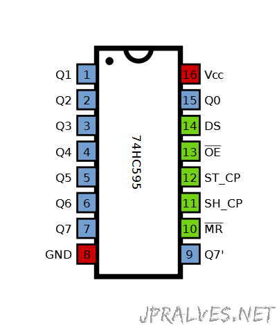
The ‘HC595 devices contain an 8-bit serial-in, parallel-out shift register that feeds an 8-bit D-type storage register. The storage register has parallel 3-state outputs. Separate clocks are provided for both the shift and storage register. The shift register has a direct overriding clear (SRCLR) input, serial (SER) input, and serial outputs for cascading. When the output-enable (OE) input is high, the outputs are in the high-impedance state. Both the shift register clock (SRCLK) and storage register clock (RCLK) are positive-edge triggered. If both clocks are connected together, the shift register always is one clock pulse ahead of the storage register.
| Pin | Name | Function |
|---|---|---|
| PINS 1-7, 15 | Q0 ” Q7 | Output Pins |
| PIN 8 | GND | Ground, Vss |
| PIN 9 | Q7” | Serial Out |
| PIN 10 | MR | Master Reclear, active low |
| PIN 11 | SH_CP | Shift register clock pin |
| PIN 12 | ST_CP | Storage register clock pin (latch pin) |
| PIN 13 | OE | Output enable, active low |
| PIN 14 | DS | Serial data input |
| PIN 16 | Vcc | Positive supply voltage |
Circuit

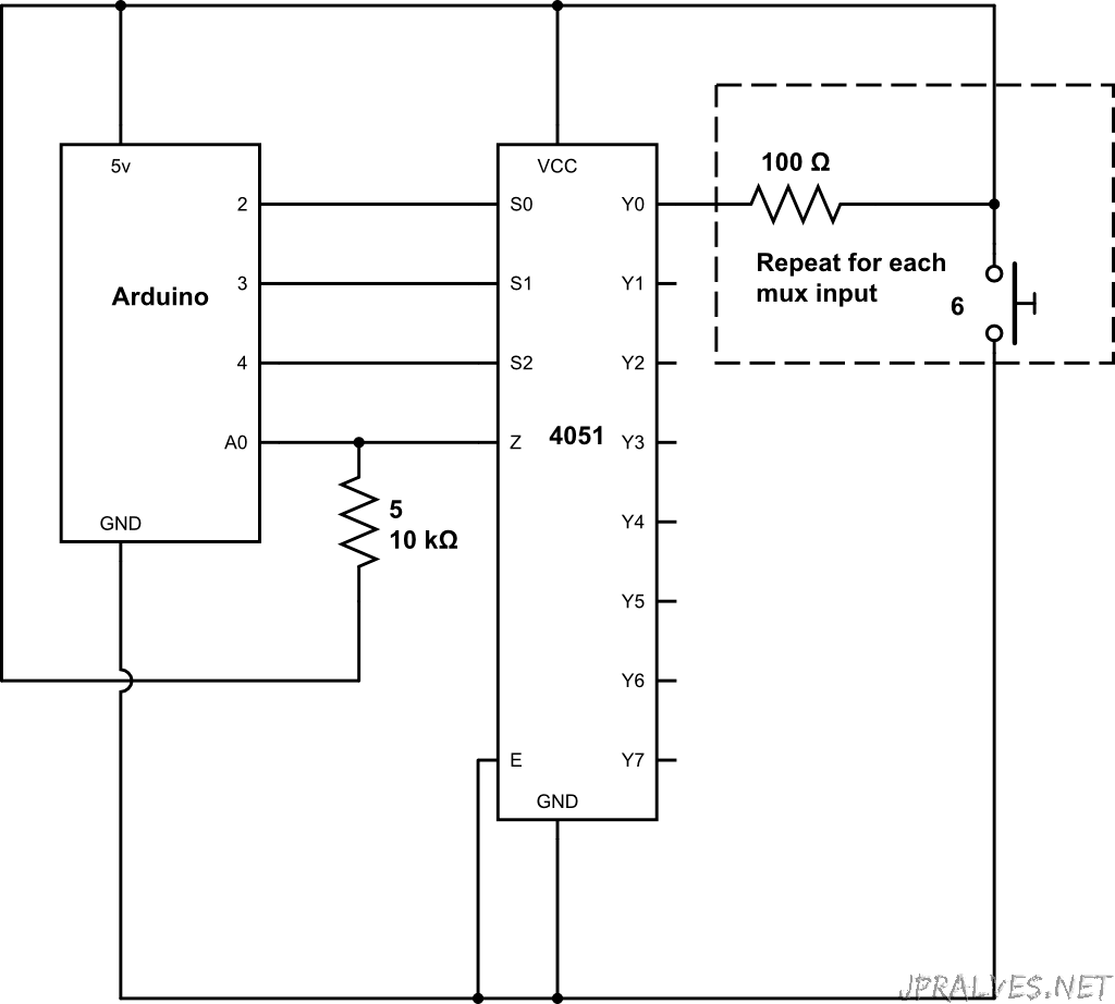
CD4051BE - CMOS Single 8-Channel Analog Multiplexer/Demultiplexer with Logic-Level Conversion

The CD4051B is a single 8-Channel multiplexer having three binary control inputs, A, B, and C, and an inhibit input. The three binary signals select 1 of 8 channels to be turned on, and connect one of the 8 inputs to the output.
The CD4052B is a differential 4-Channel multiplexer having two binary control inputs, A and B, and an inhibit input. The two binary input signals select 1 of 4 pairs of channels to be turned on and connect the analog inputs to the outputs.
The CD4053B is a triple 2-Channel multiplexer having three separate digital control inputs, A, B, and C, and an inhibit input. Each control input selects one of a pair of channels which are connected in a single-pole, double-throw configuration.
Circuit
TLC5940NT - 16-Channel LED Driver w/EEprom DOT Correction & Grayscale PWM Control
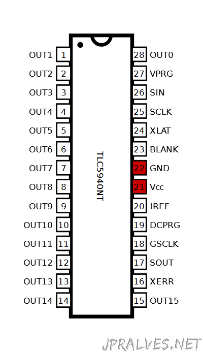
The TLC5940 is a 16-channel, constant-current sink LED driver. Each channel has an individually adjustable 4096-step grayscale PWM brightness control and a 64-step, constant-current sink (dot correction). The dot correction adjusts the brightness variations between LED channels and other LED drivers. The dot correction data is stored in an integrated EEPROM. Both grayscale control and dot correction are accessible via a serial interface. A single external resistor sets the maximum current value of all 16 channels.
The TLC5940 features two error information circuits. The LED open detection (LOD) indicates a broken or disconnected LED at an output terminal. The thermal error flag (TEF) indicates an overtemperature condition.
Circuit
LM335Z - Precision Temperature Sensors

The LM135 series are precision, easily-calibrated, integrated circuit temperature sensors. Operating as a 2-terminal zener, the LM135 has a breakdown voltage directly proportional to absolute temperature at +10 mV/°K. With less than 1Ω dynamic impedance the device operates over a current range of 400 μA to 5 mA with virtually no change in performance. When calibrated at 25°C the LM135 has typically less than 1°C error over a 100°C temperature range. Unlike other sensors the LM135 has a linear output.
Applications for the LM135 include almost any type of temperature sensing over a −55°C to 150°C temperature range. The low impedance and linear output make interfacing to readout or control circuitry especially easy.
The LM135 operates over a −55°C to 150°C temperature range while the LM235 operates over a −40°C to 125°C temperature range. The LM335 operates from −40°C to 100°C. The LM135/LM235/LM335 are available packaged in hermetic TO transistor packages while the LM335 is also available in plastic TO-92 packages.
Circuit and Code
//initializes/defines the output pin of the LM335 temperature sensor
int outputpin= 0;
//this sets the ground pin to LOW and the input voltage pin to high
void setup() {
Serial.begin(9600);
}

//main loop
void loop() {
int rawvoltage= analogRead(outputpin);
float millivolts= (rawvoltage/1024.0) * 5000;
float kelvin= (millivolts/10);
float celsius= kelvin - 273.15;
float fahrenheit= ((celsius * 9)/5 +32);

Serial.print(kelvin);
Serial.println(" degrees Kelvin");

serial.print(celsius);
Serial.println(" degrees Celsius");

serial.print(fahrenheit);
Serial.println(" degrees Fahrenheit");

delay(3000);
}
OPA170 - 36V, microPower, Rail-to-Rail Output, General Purpose Op Amp
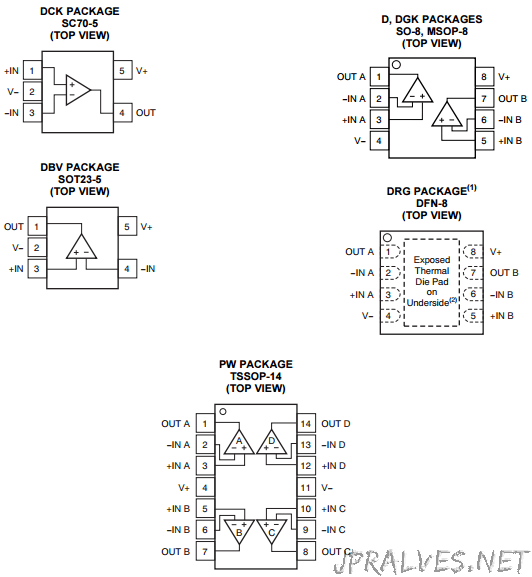
The OPA170, OPA2170 and OPA4170 (OPAx170) are a family of 36V, single-supply, low-noise operational amplifiers that feature micro packages with the ability to operate on supplies ranging from +2.7V (±1.35V) to +36V (±18V). They offer good offset, drift, and bandwidth with low quiescent current. The single, dual, and quad versions all have identical specifications for maximum design flexibility. Unlike most op amps, which are specified at only one supply voltage, the OPAx170 family of op amps is specified from +2.7V to +36V. Input signals beyond the supply rails do not cause phase reversal. The OPAx170 family is stable with capacitive loads up to 300pF. The input can operate 100mV below the negative rail and within 2V of the positive rail for normal operation. Note that these devices can operate with full rail-to-rail input 100mV beyond the positive rail, but with reduced performance within 2V of the positive rail. The OPA170 is available in SOT553, SOT23-5, and SO-8 packages. The dual OPA2170 comes in VSSOP-8, MSOP-8, and SO-8 packages. The quad OPA4170 is offered in TSSOP-14 and SO-14 packages. The OPAx170 op amps are specified from –40°C to +125°C.
Circuit

OPA314 - 3MHz, Low-Power, Low-Noise, RRI/O, 1.8V CMOS Operational Amplifier

The OPA314 family of single-, dual-, and quad-channel operational amplifiers represents a new generation of low-power, general-purpose CMOS amplifiers. Rail-to-rail input and output swings, low quiescent current (150 µA typ at 5.0 VvertAlign;valsubscript;None
S) combined with a wide bandwidth of 3 MHz, and very low noise (14 nV/√Hzat 1 kHz) make this family very attractive for a variety of battery-powered applications that require a good balance between cost and performance. The low input bias current supports applications with mega-ohm source impedances.
The robust design of the OPA314 devices provides ease-of-use to the circuit designer: unity-gain stability with capacitive loads of up to 300 pF, an integrated RF/EMI rejection filter, no phase reversal in overdrive conditions, and high electrostatic discharge (ESD) protection (4-kV HBM).
These devices are optimized for low-voltage operation as low as +1.8 V (±0.9 V) and up to +5.5 V (±2.75 V), and are specified over the full extended temperature range of –40°C to +125°C.
The OPA314 (single) is available in both SC70-5 and SOT23-5 packages. The OPA2314 (dual) is offered in SO-8, MSOP-8, and DFN-8 packages. The quad-channel OPA4314 is offered in a TSSOP-14 package.
Circuit
OPA313 - 1-MHz, Micropower, Low-Noise, Rail-to-Rail I/O 1.8-V Operational Amplifier
The OPA313 family of single-, dual-, and quad-channel op amps represents a new generation of low-cost, general purpose, micro-power operational amplifiers. Featuring rail-to-rail input and very low noise (25 nV/√Hz at 1 kHz) makes this family very attractive for a variety of battery-powered applications that require a good balance between cost and performance. The low input bias current supports those op amps to be used in applications with megaohm source impedances.
The robust design of the OPA313 devices provides ease-of-use to the circuit designer: unity-gain stability with capacitive loads of up to 150 pF, integrated RF/EMI rejection filter, no phase reversal in overdrive conditions, and high electrostatic discharge (ESD) protection (4-kV HBM).
These devices are optimized for operation at voltages as low as +1.8 V (±0.9 V) and up to +5.5 V (±2.75 V), and are specified over the extended temperature range of –40°C to +125°C.
The OPA313 (single) is available in both SC70-5 and SOT23-5 packages. The OPA2313 (dual) is offered in SO-8, MSOP-8, and DFN-8 packages. The quad-channel OPA4313 is offered in a TSSOP-14 package.U.S.Electronics
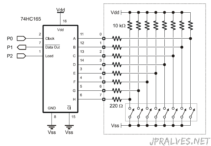
SN74HC165 - 8-Bit Parallel-Load Shift Registers
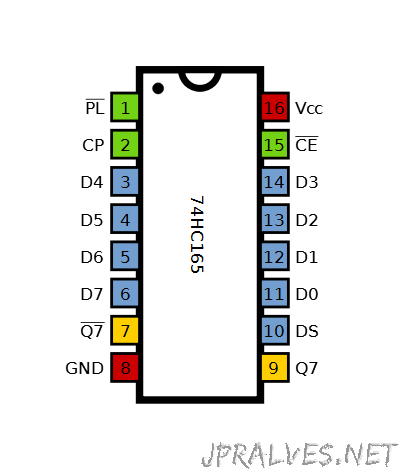
The ’HC165 devices are 8-bit parallel-load shift registers that, when clocked, shift the data toward a serial (QvertAlign;valsubscript;None
H) output. Parallel-in access to each stage is provided by eight individual direct data (A−H) inputs that are enabled by a low level at the shift/load (SH/LD) input. The ’HC165 devices also feature a clock-inhibit (CLK INH) function and a complementary serial (QH) output.
Clocking is accomplished by a low-to-high transition of the clock (CLK) input while SH/LD is held high and CLK INH is held low. The functions of CLK and CLK INH are interchangeable. Since a low CLK and a low-to-high transition of CLK INH also accomplish clocking, CLK INH should be changed to the high level only while CLK is high. Parallel loading is inhibited when SH/LD is held high. While SH/LD is low, the parallel inputs to the register are enabled independently of the levels of the CLK, CLK INH, or serial (SER) inputs.
Circuit
SN74HC04N - HEX INVERTERS
The ’HC04 devices contain six independent inverters. They perform the Boolean function Y = A in positive logic.

Circuit
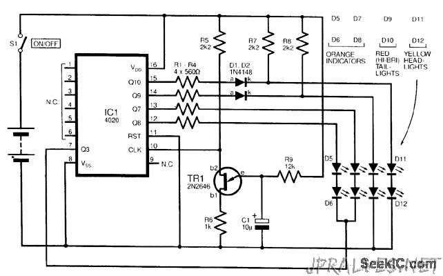
CD4020BE - CMOS 14-Stage Ripple-Carry Binary Counter/Divider
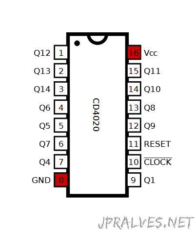
CD4020B, CD4024B, and CD4040B are ripple-carry binary counters. All counter stages are master-slave flip-flops. The state of a counter advances one count on the negative transition of each input pulse; a high level on the RESET line resets the counter to its all zeros state. Schmitt trigger action on the input-pulse line permits unlimited rise and fall times. All inputs and outputs are buffered.
The CD4020B and CD4040B types are supplied in 16-lead hermetic dual-in-line ceramic packages (F3A suffix), 16-lead dual-in-line plastic packages (E suffix), 16-lead small-outline packages (NSR suffix), and 16-lead thin shrink small-outline packages (PW and PWR suffixes). The CD4040B type also is supplied in 16-lead small-outline packages (M and M96 suffixes).
The CD4024B types are supplied in 14-lead hermetic dual-in-line ceramic packages (F3A suffix), 14-lead dual-in-line plastic packages (E suffix), 14-lead small-outline packages (M, MT, M96, and NSR suffixes), and 14-lead thin shrink small-outline packages (PW and PWR suffixes).
Circuit
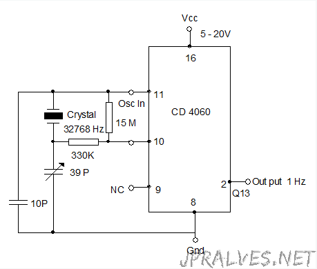
CD4060BN - CMOS 14-Stage Ripple-Carry Binary Counter/Divider and Oscillator
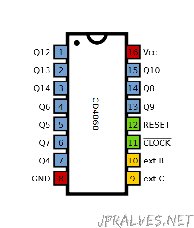
CD4060B consists of an oscillator section and 14 ripple-carry binary counter stages. The oscillator configuration allows design of either RC or crystal oscillator circuits. A RESET input is provided which resets the counter to the all-O’s state and disables the oscillator. A high level on the RESET line accomplishes the reset function. All counter stages are master-slave flip-flops. The state of the counter is advanced one step in binary order on the negative transition of 
O). All inputs and outputs are fully buffered. Schmitt trigger action on the input-pulse line permits unlimited input-pulse rise and fall times.
The CD4060B-series types are supplied in 16-lead hermetic dual-in-line ceramic packages (F3A suffix), 16-lead dual-in-line plastic packages (E suffix), 16-lead small-outline packages (M, M96, MT and NSR suffixes), and 16-lead thin shrink small-outline packages (PW and PWR suffixes).
Circuit
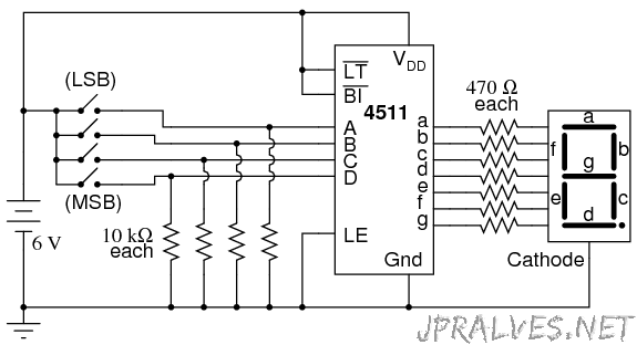
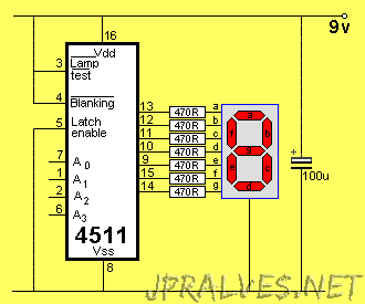
CD4511B - CMOS BCD-to-7-Segment LED Latch Decoder Drivers
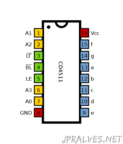
CD4511B types are BCD-to-7-segment latch decoder drivers constructed with CMOS logic and n-p-n bipolar transistor output devices on a single monolithic structure. These devices combine the low quiescent power dissipation and high noise immunity features of RCA CMOS with n-p-n bipolar output transistors capable of sourcing up to 25 MA. This capability allows the CD4511B types to drive LED’s and other displays directly.
Lamp Test (LT)\, Blanking (BL)\, and Latch Enable or Strobe inputs are provided to test the display, shut off or intensity-modulate it, and store or strobe a BCD code, respectively. Several different signals may be multiplexed and displayed when external multiplexing circuitry is used.
The CD4511B types are supplied in 16-lead hermetic dual-in-line ceramic packages (F3A suffix), 16-lead dual-in-line plastic packages (E suffix), 16-lead small-outline packages (NSR suffix), and 16-lead thin shrink small-outline packages (PW and PWR suffixes).
These devices are similar to the type MC14511.
Circuit
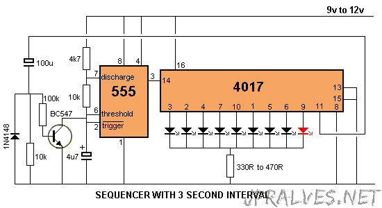
CD4017BE - CMOS Decade Counter with 10 Decoded Outputs
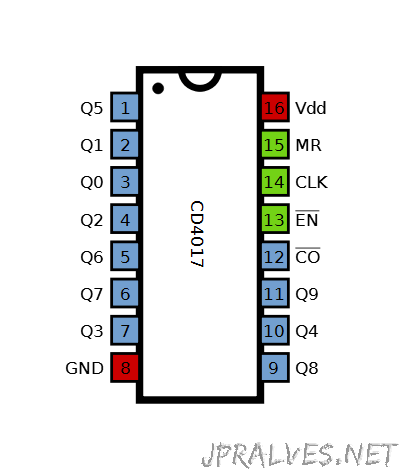
CD4017B and CD4022B are 5-stage and 4-stage Johnson counters having 10 and 8 decoded outputs, respectively. Inputs include a CLOCK, a RESET, and a CLOCK INHIBIT signal. Schmitt trigger action in the CLOCK input circuit provides pulse shaping that allows unlimited clock input pulse rise and fall times.
These counters are advanced one count at the positive clock signal transition if the CLOCK INHIBIT signal is low. Counter advancement via the clock line is inhibited when the CLOCK INHIBIT signal is high. A high RESET signal clears the counter to its zero count. Use of the Johnson counter configuration permits high-speed operation, 2-input decode-gating and spike-free decoded outputs. Anti-lock gating is provided, thus assuring proper counting sequence. The decoded output are normally low and go high only at their respective decoded time slot. Each decoded output remains high for one full clock cycle. A CARRY-OUT signal completes on cycle every 10 clock input cycles in the CD4017B or every 8 clock input cycles in the CD4022B and is used to ripple-clock the succeeding device in a multi-device counting chain.
The CD4017B and CD4022B types are supplied in 16-lead hermetic dual-in-line ceramic packages (F3A suffix), 16-lead dual-in-line plastic package (E suffix), 16-lead small-outline packages (NSR suffix), and 16-lead thin shrink small-outline packages (PW and PWR suffixes). The CD4017B types also are supplied in 16-lead small-outline packages (M and M96 suffixes).
Circuit
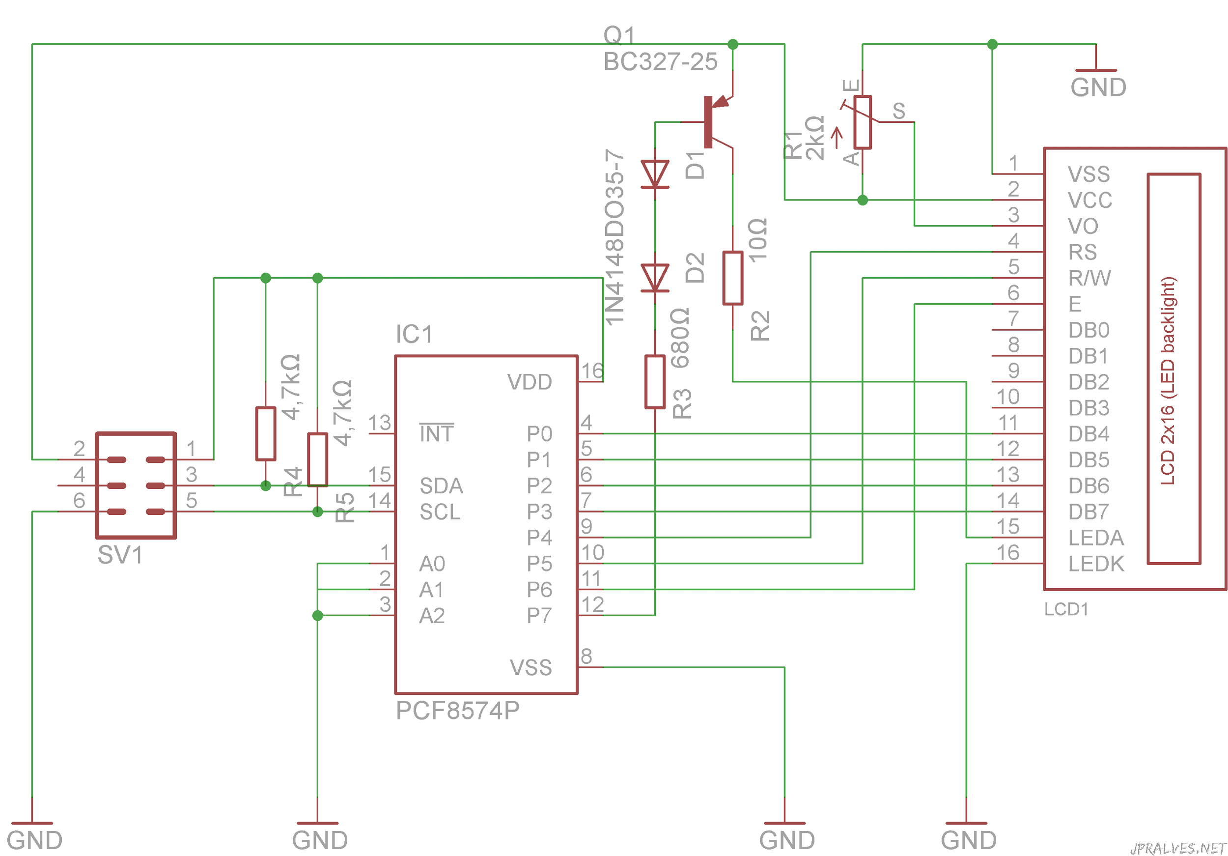
PCF8574AN - Remote 8-Bit I/O Expander for I2C-Bus
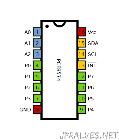
This 8-bit input/output (I/O) expander for the two-line bidirectional bus (I2C) is designed for 2.5-V to 6-V VCC operation.
The PCF8574A provides general-purpose remote I/O expansion for most microcontroller families via the I2C interface [serial clock (SCL), serial data (SDA)].The device features an 8-bit quasi-bidirectional I/O port (P0-P7), including latched outputs with high-current drive capability for directly driving LEDs. Each quasi-bidirectional I/O can be used as an input or output without the use of a data-direction control signal. At power on, the I/Os are high. In this mode, only a current source to VCC is active. An additional strong pullup to VCC allows fast rising edges into heavily loaded outputs. This device turns on when an output is written high and is switched off by the negative edge of SCL. The I/Os should be high before being used as inputs.The PCF8574A provides an open-drain output (INT) that can be connected to the interrupt input of a microcontroller. An interrupt is generated by any rising or falling edge of the port inputs in the input mode. After time, tiv, INT is valid. Resetting and reactivating the interrupt circuit is achieved when data on the port is changed to the original setting or data is read from, or written to, the port that generated the interrupt. Resetting occurs in the read mode at the acknowledge bit after the rising edge of the SCL signal, or in the write mode at the acknowledge bit after the high-to-low transition of the SCL signal. Interrupts that occur during the acknowledge clock pulse can be lost (or be very short) due to the resetting of the interrupt during this pulse. Each change of the I/Os after resetting is detected and, after the next rising clock edge, is transmitted as INT. Reading from, or writing to, another device does not affect the interrupt circuit.By sending an interrupt signal on this line, the remote I/O can inform the microcontroller if there is incoming data on its ports without having to communicate via the I2C bus. Therefore, the PCF8574A can remain a simple slave device.
Circuit
SN74HC14N - Hex Schmitt-Trigger Inverters

These Schmitt-trigger devices contain six independent inverters. They perform the Boolean function Y = A in positive logic.
Circuit
CD4028B - CMOS BCD-to-Decimal or Binary-to-Octal Decoders/Drivers
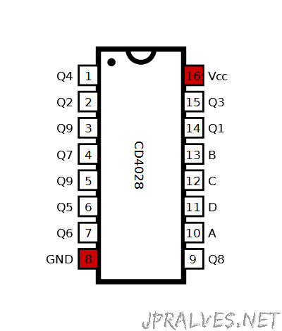
CD4028 types are BCD-to-decimal or binary-to-octal decoders consisting of buffering on all 4 inputs, decoding-logic gates, and 10 output buffers. A BCD code applied to the four input, A to D, results in a high level at the selected one of 10 decimal decoded outputs. Similarly, a 3-bit binary code applied to inputs A through C is decoded in octal code at output 0 to 7 if D = “0”. High drive capability is provided at all outputs to enhance dc and dynamic performance in high fan-out applications.
The CD4028B-Series types are supplied in 16-lead hermetic dual-in-line ceramic packages (F3A suffix), 16-lead dual-in-line plastic packages (E suffix), 16-lead small-outline packages (M, M96, MT and NSR suffixes), and 16-lead thin shrink small-outline packages (PW and PWR suffixes).
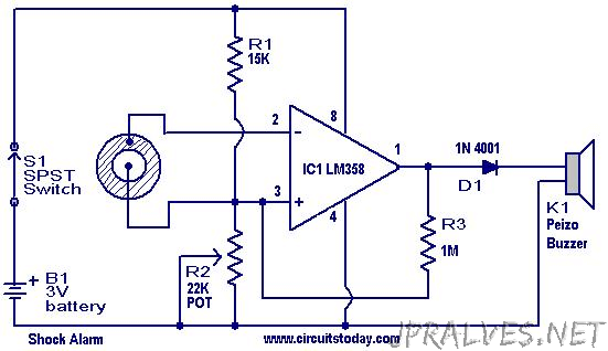
LM358 - Dual Operational Amplifiers
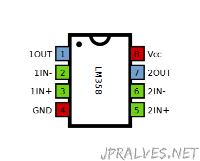
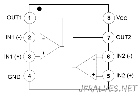
These devices consist of two independent, high-gain frequency-compensated operational amplifiers designed to operate from a single supply over a wide range of voltages. Operation from split supplies also is possible if the difference between the two supplies is 3 V to 32 V (3 V to 26 V for the LM2904), and VCC is at least 1.5 V more positive than the input common-mode voltage. The low supply-current drain is independent of the magnitude of the supply voltage.
Applications include transducer amplifiers, dc amplification blocks, and all the conventional operational amplifier circuits that now can be implemented more easily in single-supply-voltage systems. For example, these devices can be operated directly from the standard 5-V supply used in digital systems and easily can provide the required interface electronics without additional ±5-V supplies.
Circuit
CD74HC238 - High Speed CMOS Logic 3-to-8 Line Decoder Demultiplexer Inverting and Non-Inverting
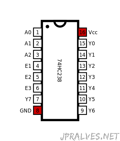
The ’HC138, ’HC238, ’HCT138, and ’HCT238 are high speed silicon gate CMOS decoders well suited to memory address decoding or data routing applications. Both circuits feature low power consumption usually associated with CMOS circuitry, yet have speeds comparable to low power Schottky TTL logic. Both circuits have three binary select inputs (A0, A1 and A2). If the device is enabled, these inputs determine which one of the eight normally high outputs of the HC/HCT138 series will go low or which of the normally low outputs of the HC/HCT238 series will go high.
Two active low and one active high enables (E1\, E2\, and E3) are provided to ease the cascading of decoders. The decoder’s 8 outputs can drive 10 low power Schottky TTL equivalent loads.
Circuit
LM2940 - 1A Low Dropout Regulator
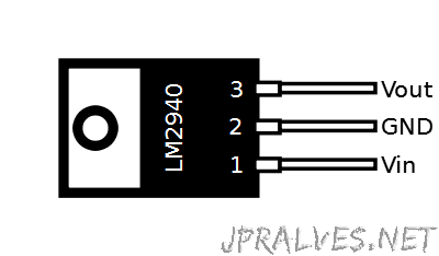
The LM2940-N/LM2940C positive voltage regulator features the ability to source 1A of output current with a dropout voltage of typically 0.5V and a maximum of 1V over the entire temperature range. Furthermore, a quiescent current reduction circuit has been included which reduces the ground current when the differential between the input voltage and the output voltage exceeds approximately 3V. The quiescent current with 1A of output current and an input-output differential of 5V is therefore only 30 mA. Higher quiescent currents only exist when the regulator is in the dropout mode (VIN − VOUT ≤ 3V).
Designed also for vehicular applications, the LM2940-N/LM2940C and all regulated circuitry are protected from reverse battery installations or 2-battery jumps. During line transients, such as load dump when the input voltage can momentarily exceed the specified maximum operating voltage, the regulator will automatically shutdown to protect both the internal circuits and the load. The LM2940/LM2940C cannot be harmed by temporary mirror-image insertion. Familiar regulator features such as short circuit and thermal overload protection are also provided.
Circuit: Typical application
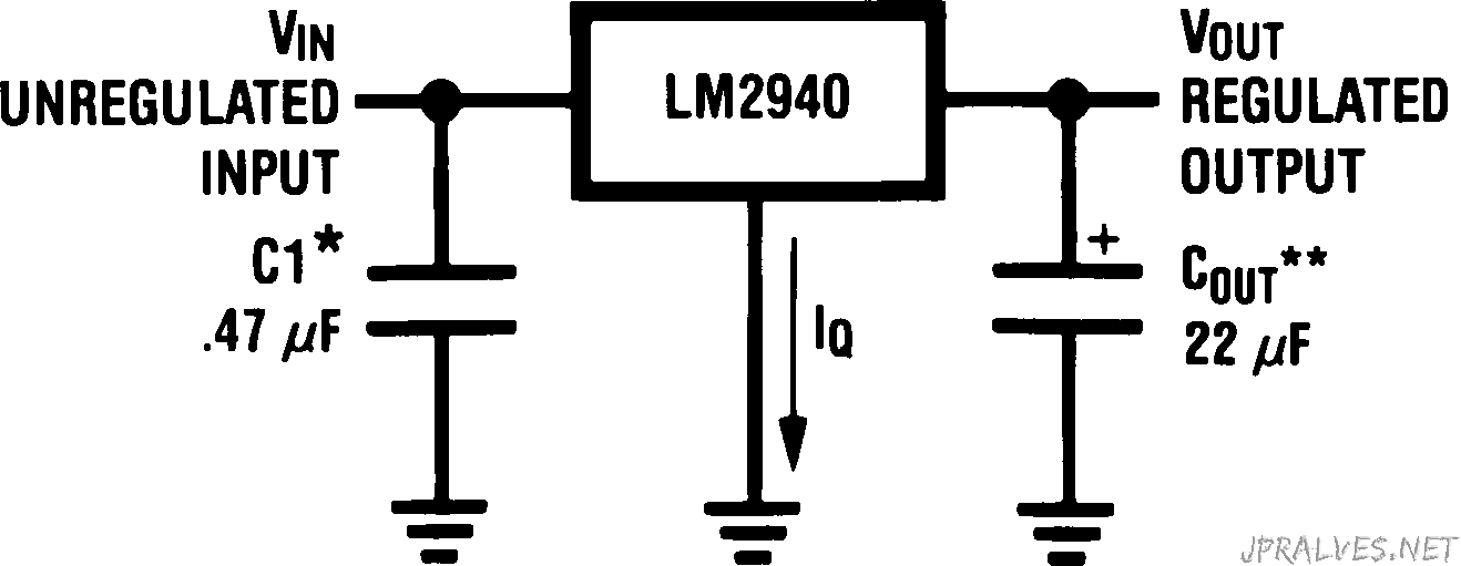
Required if regulator is located far from power supply filter.
*COUT must be at least 22 μF to maintain stability. May be increased without bound to maintain regulation during transients. Locate as close as possible to the regulator. This capacitor must be rated over the same operating temperature range as the regulator and the ESR is critical; see curve.
CD4520B - CMOS Dual Binary Up-Counter

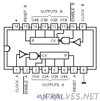
CD4518 Dual BCD Up-Counter and CD4520 Dual Binary Up-Counter each consist of two identical, internally synchronous 4-stage counters. The counter stages are D-type flip-flops having interchangeable CLOCK and ENABLE lines for incrementing on either the positive-going or negative-going transition. For single-unit operation the ENABLE input is maintained high and the counter advances on each positive-going transition of the CLOCK. The counters are cleared by high levels on their RESET lines.
The counter can be cascaded in the ripple mode by connecting Q4 to the enable input of the subsequent counter while the CLOCK input of the latter is held low.
The CD4518B and CD4520B types are supplied in 16-lead hermetic dual-in-line ceramic packages (F3A suffix), 16-lead dual-in-line plastic packages (E suffix), 16-lead small-outline packages (M, M96, and NSR suffixes), and 16-lead thin shrink small-outline packages (PW and PWR suffixes).
TLC5916IN - 8-Bit Constant-Current LED Sink Driver
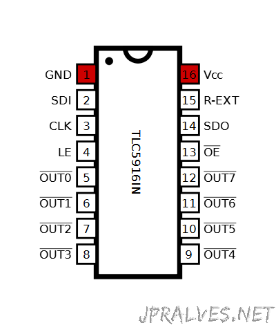
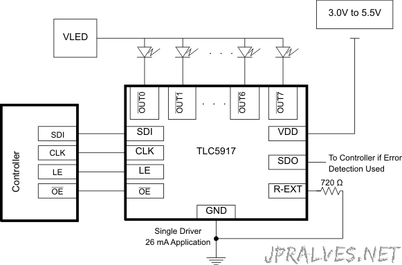
The TLC5916 / TLC5917 Constant-Current LED Sink Drivers are designed to work alone or cascaded. Since each output is independently controlled, they can be programmed to be on or off by the user. The high LED voltage (VLED) allows for the use of a single LED per output or multiple LEDs on a single string. With independently controlled outputs supplied with constant current, the LEDs can be combined in parallel to create higher currents on a single string. The constant sink current for all channels is set through a single external resistor. This allows different LED drivers in the same application to sink various currents which provides optional implementation of multi-color LEDs. An additional advantage of the independent outputs is the ability to leave unused channels floating. The flexibility of the TLC5916 / TLC5917 LED drivers is ideal for applications such as (but not limited to): 7-segment displays, scrolling single color displays, gaming machines, white goods, video billboards and video panels.
Features
- Eight Constant-Current Output Channels
- Output Current Adjusted Through Single External Resistor
- Constant Output Current Range: 3 mA to 120 mA per Channel
- Constant Output Current Invariant to Load Voltage Change
- Open Load, Short Load and Overtemperature Detection
- 256-Step Programmable Global Current Gain
- Excellent Output Current Accuracy:
- Between Channels: < ±3% (Max)
- Between ICs: < ±6% (Max)
- Fast Response of Output Current
- 30-MHz Clock Frequency
- Schmitt-Trigger Input
- 3.3-V or 5-V Supply Voltage
- Maximum LED Voltage 20-V
- Thermal Shutdown for Overtemperature Protection
- APPLICATIONS
- General LED Lighting Applications
- LED Display Systems
- LED Signage
- Automotive LED Lighting
- White Goods
- Gaming Machines/Entertainment
OPA2344PA - Low Power, Single-Supply, Rail-To-Rail Operational Amplifiers MicroAmplifier(TM)*_
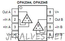
The OPA344 and OPA345 series rail-to-rail CMOS operational amplifiers are designed for precision, low-power, miniature applications. The OPA344 is unity gain stable, while the OPA345 is optimized for gains greater than or equal to five, and has a gain-bandwidth product of 3MHz.
The OPA344 and OPA345 are optimized to operate on a single supply from 2.5V and up to 5.5V with an input common-mode voltage range that extends 300mV beyond the supplies. Quiescent current is only 250µA (max).
Rail-to-rail input and output make them ideal for driving sampling analog-to-digital converters. They are also well suited for general purpose and audio applications and providing I/V conversion at the output of D/A converters. Single, dual and quad versions have identical specs for design flexibility.
A variety of packages are available. All are specified for operation from –40°C to 85°C.
Circuit
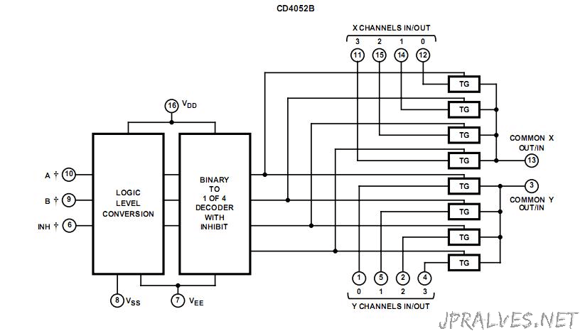
CD4052BE - CMOS Differential 4-Channel Analog Multiplexer/Demultiplexer with Logic-Level Conversion

The CD4051B, CD4052B, and CD4053B analog multiplexers are digitally-controlled analog switches having low ON impedance and very low OFF leakage current. Control of analog signals up to 20VP-P can be achieved by digital signal amplitudes of 4.5V to 20V (if VDD–VSS = 3V, a VDD–VEE of up to 13V can be controlled; for VDD–VEE level differences above 13V, a VDD–VSS of at least 4.5V is required). For example, if VDD = +4.5V, VSS = 0V, and VEE = –13.5V, analog signals from –13.5V to +4.5V can be controlled by digital inputs of 0V to 5V. These multiplexer circuits dissipate extremely low quiescent power over the full VDD–VSS and VDD–VEE supply-voltage ranges, independent of the logic state of the control signals. When a logic “1” is present at the inhibit input terminal, all channels are off.
The CD4052B is a differential 4-Channel multiplexer having two binary control inputs, A and B, and an inhibit input. The two binary input signals select 1 of 4 pairs of channels to be turned on and connect the analog inputs to the outputs.
When these devices are used as demultiplexers, the “CHANNEL IN/OUT” terminals are the outputs and the “COMMON OUT/IN” terminals are the inputs.
Features
- Wide Range of Digital and Analog Signal Levels
- Digital…3V to 20V
- Analog…≤20VP-P
- Low ON Resistance, 125Ω (Typ) Over 15VP-P
- Signal Input Range for VDD–VEE = 18V
- High OFF Resistance, Channel Leakage of ±100pA (Typ) at VDD–VEE = 18V
- Logic-Level Conversion for Digital Addressing Signals of 3V to 20V (VDD–VSS = 3V to 20V) to Switch Analog Signals to 20VP-P (VDD–VEE = 20V)
- Matched Switch Characteristics, rON = 5Ω (Typ) for VDD–VEE = 15V
- Very Low Quiescent Power Dissipation Under All Digital-Control Input and Supply Conditions, 0.2µW (Typ) at VDD–VSS = VDD–VEE = 10V
- Binary Address Decoding on Chip
- 5V, 10V and 15V Parametric Ratings
- 10% Tested for Quiescent Current at 20V
- Maximum Input Current of 1µA at 18V Over Full Package
- Temperature Range, 100nA at 18V and 25°C
- Break-Before-Make Switching Eliminates Channel Overlap
- Applications
- Analog and Digital Multiplexing and Demultiplexing
- A/D and D/A Conversion
- Signal Gating
Circuit
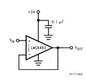
LMC6482IN - CMOS Dual Rail-to-Rail Input and Output Operational Amplifier
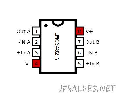
The LMC6482 provides a common-mode range that extends to both supply rails. This rail-to-rail performance combined with excellent accuracy, due to a high CMRR, makes it unique among rail-to-rail input amplifiers.
It is ideal for systems, such as data acquisition, that require a large input signal range. The LMC6482 is also an excellent upgrade for circuits using limited common-mode range amplifiers such as the TLC272 and TLC277.
Maximum dynamic signal range is assured in low voltage and single supply systems by the LMC6482’s rail-to-rail output swing. The LMC6482’s rail-to-rail output swing is ensured for loads down to 600Ω.
Ensured low voltage characteristics and low power dissipation make the LMC6482 especially well-suited for battery-operated systems.
LMC6482 is also available in VSSOP package which is almost half the size of a SOIC-8 device. See the LMC6484 data sheet for a Quad CMOS operational amplifier with these same features.
Features
- (Typical Unless Otherwise Noted)
- Rail-to-Rail Input Common-Mode Voltage Range (Ensured Over Temperature)
- Rail-to-Rail Output Swing (within 20mV of Supply Rail, 100kΩ Load)
- Ensured 3V, 5V and 15V Performance
- Excellent CMRR and PSRR: 82dB
- Ultra Low Input Current: 20fA
- High Voltage Gain (RL = 500kΩ): 130dB
- Specified for 2kΩ and 600Ω Loads
- Available in VSSOP Package
Circuit
LMC6484IN - CMOS Quad Rail to Rail Input and Output Operational Amplifier
The LMC6484 provides a common-mode range that extends to both supply rails. This rail-to-rail performance combined with excellent accuracy, due to a high CMRR, makes it unique among rail-to-rail input amplifiers.
It is ideal for systems, such as data acquisition, that require a large input signal range. The LMC6484 is also an excellent upgrade for circuits using limited common-mode range amplifiers such as the TLC274 and TLC279.
Maximum dynamic signal range is assured in low voltage and single supply systems by the LMC6484’s rail-to-rail output swing. The LMC6484’s rail-to-rail output swing is guaranteed for loads down to 600[Ohm].
Guaranteed low voltage characteristics and low power dissipation make the LMC6484 especially well-suited for battery-operated systems.
See the LMC6482 data sheet for a Dual CMOS operational amplifier with these same features.
Features
- (Typical unless otherwise noted)
- Rail-to-Rail Input Common-Mode Voltage Range (Guaranteed Over Temperature)
- Rail-to-Rail Output Swing (within 20 mV of supply rail, 100 k[Ohm] load)
- Guaranteed 3V, 5V and 15V Performance
- Excellent CMRR and PSRR: 82 dB
- Ultra Low Input Current: 20 fA
- High Voltage Gain (RL = 500 k[Ohm]): 130 dB
- Specified for 2 k[Ohm] and 600[Ohm] loads
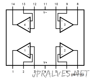
LM393 - Dual Differential Comparator
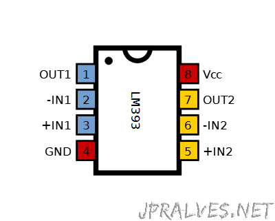
These devices consist of two independent voltage comparators that are designed to operate from a single power supply over a wide range of voltages. Operation from dual supplies also is possible as long as the difference between the two supplies is 2 V to 36 V, and VCC is at least 1.5 V more positive than the input common-mode voltage. Current drain is independent of the supply voltage. The outputs can be connected to other open-collector outputs to achieve wired-AND relationships.
The LM193 is characterized for operation from −55°C to 125°C. The LM293 and LM293A are characterized for operation from −25°C to 85°C. The LM393 and LM393A are characterized for operation from 0°C to 70°C. The LM2903 is characterized for operation from −40°C to 125°C.
Circuit: LM393 Comparator Night Light Circuit
(Link)
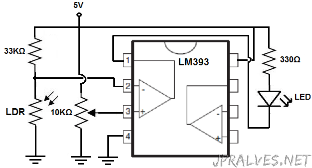
Components Needed:
- LM393 IC
- Photoresistor
- 33KΩ Resistor
- 330Ω Resistor
- Potentiometer (1KΩ-20KΩ)
- LED
- 3 ‘AA’ batteries or DC power supply
This comparator circuit then compares this reference voltage with the voltage produced from the voltage divider between the photoresistor and the 33KΩ resistor. It’s a really simple concept. When the photoresistor is exposed to bright light, its resistance falls well below 30KΩ. Therefore, most of the voltage gets allocated to the 33KΩ resistor and little goes across the photoresistor. Thus, the voltage produced by the voltage divider is less than the reference voltage. Therefore, the output is drawn to GND, which means the LED is not powered. However, during darkness, the photoresistor has a very high resistance, so most of the voltage gets allocated across it. Thus, the voltage produced from the divider circuit is above the reference voltage. Thus, the output is drawn high to Vcc, and the LED turns on.
And this is the basis of a comparator circuit.
TL494 - Pulse-Width-Modulation Control Circuits
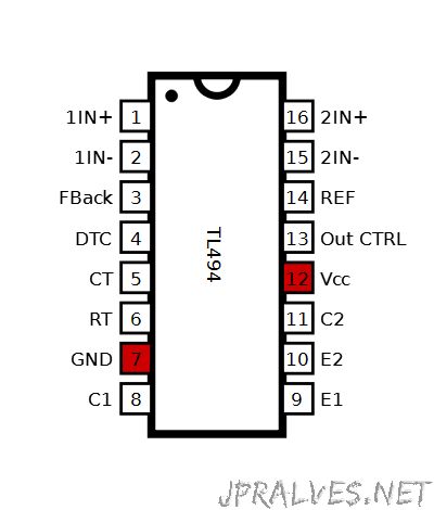
The TL494 device incorporates all the functions required in the construction of a pulse-width-modulation (PWM) control circuit on a single chip. Designed primarily for power-supply control, this device offers the flexibility to tailor the power-supply control circuitry to a specific application.
The TL494 device contains two error amplifiers, an on-chip adjustable oscillator, a dead-time control (DTC) comparator, a pulse-steering control flip-flop, a 5-V, 5%-precision regulator, and output-control circuits.
The error amplifiers exhibit a common-mode voltage range from –0.3 V to VCC – 2 V. The dead-time control comparator has a fixed offset that provides approximately 5% dead time. The on-chip oscillator can be bypassed by terminating RT to the reference output and providing a sawtooth input to CT, or it can drive the common circuits in synchronous multiple-rail power supplies.
The uncommitted output transistors provide either common-emitter or emitter-follower output capability. The TL494 device provides for push-pull or single-ended output operation, which can be selected through the output-control function. The architecture of this device prohibits the possibility of either output being pulsed twice during push-pull operation.
The TL494C device is characterized for operation from 0°C to 70°C. The TL494I device is characterized for operation from -40°C to 85°C.
Circuit

SN74AHC125 - Quadruple Bus Buffer Gates With 3-State Outputs
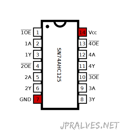
The ’AHC125 devices are quadruple bus buffer gates featuring independent line drivers with 3-state outputs. Each output is disabled when the associated output-enable (OE) input is high. When OE is low, the respective gate passes the data from the A input to its Y output.
To ensure the high-impedance state during power up or power down, OE should be tied to VCC through a pullup resistor; the minimum value of the resistor is determined by the current-sinking capability of the driver.
Features
- Operating Range 2-V to 5.5-V
- Latch-Up Performance Exceeds 250 mA Per JESD 17
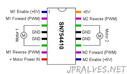
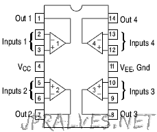
SN754410NE - Quadruple Half-H Driver
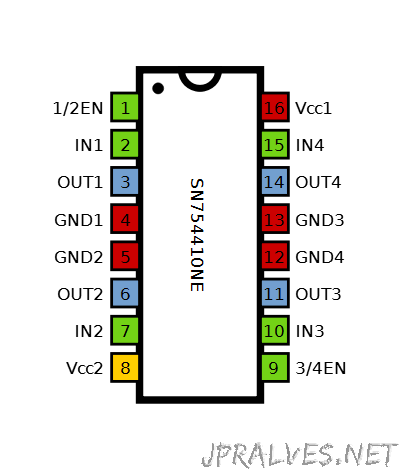
The SN754410 is a quadruple high-current half-H driver designed to provide bidirectional drive currents up to 1 A at voltages from 4.5 V to 36 V. The device is designed to drive inductive loads such as relays, solenoids, DC and bipolar stepping motors, as well as other high-current/high-voltage loads in positive-supply applications.
All inputs are compatible with TTL-and low-level CMOS logic. Each output (Y) is a complete totem-pole driver with a Darlington transistor sink and a pseudo-Darlington source. Drivers are enabled in pairs with drivers 1 and 2 enabled by 1,2EN and drivers 3 and 4 enabled by 3,4EN. When an enable input is high, the associated drivers are enabled and their outputs become active and in phase with their inputs. When the enable input is low, those drivers are disabled and their outputs are off and in a high-impedance state. With the proper data inputs, each pair of drivers form a full-H (or bridge) reversible drive suitable for solenoid or motor applications.
A separate supply voltage (VCC1) is provided for the logic input circuits to minimize device power dissipation. Supply voltage VCC2 is used for the output circuits.
The SN754410 is designed for operation from −40°C to 85°C.
Circuit
LM2901N - Low Power Low Offset Voltage Quad Comparator
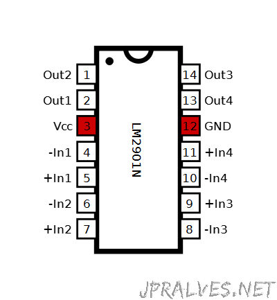
The LMx39-N series consists of four independent precision voltage comparators with an offset voltage specification as low as 2 mV maximum for all four comparators. These comparators were designed specifically to operate from a single power supply over a wide range of voltages. Operation from split power supplies is also possible and the low power supply current drain is independent of the magnitude of the power supply voltage. These comparators also have a unique characteristic in that the input common-mode voltage range includes ground, even though they are operated from a single power supply voltage.
The LMx39-N series was designed to directly interface with TTL and CMOS. When operated from both plus and minus power supplies, the devices directly interface with MOS logic – where the low power drain of the LM339 is a distinct advantage over standard comparators.
SN74LS04 - Hex inverters
These devices contain six independent inverters.
ULN2003A - High-Voltage, High-Current Darlington Transistor Arrays
The ULx200xA devices are high-voltage, high-current Darlington transistor arrays. Each consists of seven NPN Darlington pairs that feature high-voltage outputs with common-cathode clamp diodes for switching inductive loads.
The collector-current rating of a single Darlington pair is 500 mA. The Darlington pairs can be paralleled for higher current capability. Applications include relay drivers, hammer drivers, lamp drivers, display drivers (LED and gas discharge), line drivers, and logic buffers. For 100-V (otherwise interchangeable) versions of the ULx2003A devices, see the SLRS023 data sheet for the SN75468 and SN75469 devices.
The ULN2002A device is designed specifically for use with 14-V to 25-V PMOS devices. Each input of this device has a Zener diode and resistor in series to control the input current to a safe limit. The ULx2003A devices have a 2.7-kΩ series base resistor for each Darlington pair for operation directly with TTL or 5-V CMOS devices.
The ULx2004A devices have a 10.5-kΩ series base resistor to allow operation directly from CMOS devices that use supply voltages of 6 V to 15 V. The required input current of the ULx2004A device is below that of the ULx2003A devices, and the required voltage is less than that required by the ULN2002A device.
Circuit
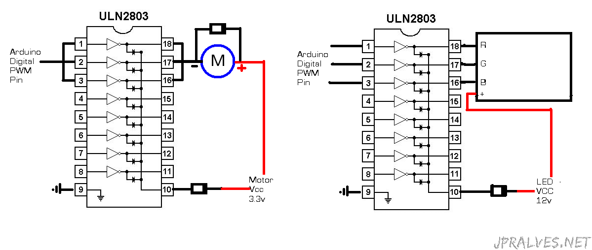
ULN2803A - Darlington Transistor Arrays
The ULN2803A device is a high-voltage, high-current Darlington transistor array. The device consists of eight NPN Darlington pairs that feature high-voltage outputs with common-cathode clamp diodes for switching inductive loads. The collector-current rating of each Darlington pair is 500 mA. The Darlington pairs may be connected in parallel for higher current capability.
Applications include relay drivers, hammer drivers, lamp drivers, display drivers (LED and gas discharge), line drivers, and logic buffers. The ULN2803A device has a 2.7-kΩ series base resistor for each Darlington pair for operation directly with TTL or 5-V CMOS devices.
Circuit
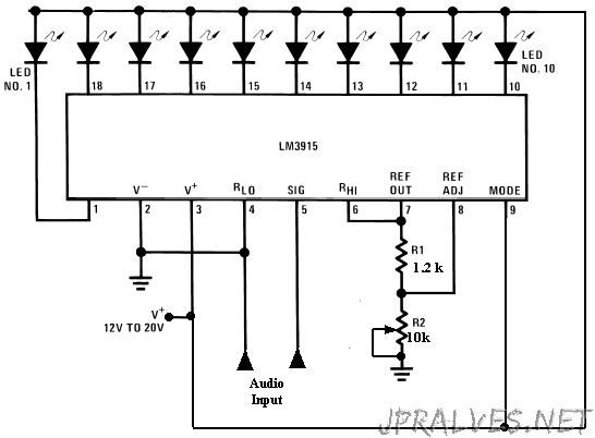
LM3915 - Dot/Bar Display Driver
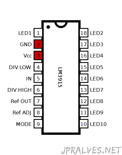
The LM3915 is a monolithic integrated circuit that senses analog voltage levels and drives ten LEDs, LCDs or vacuum fluorescent displays, providing a logarithmic 3 dB/step analog display. One pin changes the display from a bar graph to a moving dot display. LED current drive is regulated and programmable, eliminating the need for current limiting resistors. The whole display system can operate from a single supply as low as 3V or as high as 25V.
The IC contains an adjustable voltage reference and an accurate ten-step voltage divider. The high-impedance input buffer accepts signals down to ground and up to within 1.5V of the positive supply. Further, it needs no protection against inputs of ±35V. The input buffer drives 10 individual comparators referenced to the precision divider. Accuracy is typically better than 1 dB.
The LM3915’s 3 dB/step display is suited for signals with wide dynamic range, such as audio level, power, light intensity or vibration. Audio applications include average or peak level indicators, power meters and RF signal strength meters. Replacing conventional meters with an LED bar graph results in a faster responding, more rugged display with high visibility that retains the ease of interpretation of an analog display.
The LM3915 is extremely easy to apply. A 1.2V full-scale meter requires only one resistor in addition to the ten LEDs. One more resistor programs the full-scale anywhere from 1.2V to 12V independent of supply voltage. LED brightness is easily controlled with a single pot.
The LM3915 is very versatile. The outputs can drive LCDs, vacuum fluorescents and incandescent bulbs as well as LEDs of any color. Multiple devices can be cascaded for a dot or bar mode display with a range of 60 or 90 dB. LM3915s can also be cascaded with LM3914s for a linear/log display or with LM3916s for an extended-range VU meter.
Circuit
LM324 - Quadruple Operational Amplifier
These devices consist of four independent high-gain frequency-compensated operational amplifiers that are designed specifically to operate from a single supply or split supply over a wide range of voltages.
CD4047BE - Monostable Multi-vibrator CMOS LP Mono/Astable
CD4047B consists of a gatable astable multivibrator with logic techniques incorporated to permit positive or negative edge-triggered monostable multivibrator action with retriggering and external counting options.
Inputs include +TRIGGER, -TRIGGER, ASTABLE, ASTABLE\, RETRIGGER, and EXTERNAL RESET. Buffered outputs are Q\, Q and OSCILLATOR. In all modes of operation, and external capacitor must be connected between C-Timing and RC-Common terminal, and an external resistor must be connected between the R-Timing and RC-Common terminals.
Astable operation is enabled by a high level on the STABLE input or a low level on the ASTABLE\ input, or both. The period of the square wave at the Q and Q\ Outputs in this mode off operation is a function of the external components employed. “True” input pulses on the ASTABLE input or “Complement” pulses on the ASTABLE\ input allow the circuit to be used as a gatable multivibrator. The OSCILLATOR output period will be half of the Q terminal output in the astable mode. However, a 50% duty cycle is not guaranteed at this output.
The CD4047B triggers in the monostable mode when a positive-going edge occurs on the +TRIGGER-input while the -TRIGGER is held low. INput pulses may be of any duration relative to the output pulse.
If retrigger capability is desired, the RETRIGGER input is pulsed. The retriggerable mode of operation is limited to positive-going edge. The CD4047B will retrigger as long as the RETRIGGER-input is high, with or without transitions (See Fig. 34).
An external countdown option can be implemented by coupling “Q” to an external “N” counter and resetting the counter with the trigger pulse. The counter output pulse is fed back to the ASTABLE\ input and has a duration equal to N times the period of the multivibrator.
A high level on the EXTERNAL RESET input assures no output pulse during an “ON” power condition. This input can also be activated to terminate the output pulse at any tine. For monostable operation, whenever VDD is applied, and internal power-on reset circuit will clock the Q output low within one output period (tM).
The CD4047B-Series types are supplied in 14-lead hermetic dual-in-line ceramic packages (F3A suffix), 14-lead dual-in-line plastic packages (E suffix), 14-lead small outline packages (M, MT, M96, and NSR suffixes), and 14-lead thin shrink small-outline packages (PW and PWR suffixes).
Circuit
(Link)
CD4011B - CMOS Decade Up-Down Counter/Latch/Display Driver
CD40110B is a dual-clocked up/down counter with a special preconditioning circuit that allows the counter to be clocked, via positive going inputs, up or down regardless of the state or timing (within 100 ns typ.) of the other clock line.
The clock signal is fed into the control logic and Johnson counter after it is preconditioned. The outputs of the Johnson counter (which include anti-lock gating to avoid being locked at an illegal state) are fed into a latch. This data can be fed directly to the decoder through the latch or can be strobed to hold a particular count while the Johnson counter continues to be clocked. The decoder feeds a seven-segment bipolar output driver which can source up to 25 mA to drive LEDs and other displays such as low-voltage fluorescent and incandescent lamps.
A short durating negative-going pulse appears on the BORROW output when the count changes from 0 to 9 or the CARRY output when the count changes from 9 to 0. At the other times the BORROW and CARRY outputs are a logic 1.
The CARRY and BORROW outputs can be tied directly to the clock-up and clock-down lines respectively of another CD40110B for easy cascading of several counters.
The CD40110B types are supplied in 16-0lead dual-in-line ceramic packages (D and F suffixes), and 16-lead dual-in-line plastic package (E suffix), and also available in chip form, (H suffix).
Features
- Separate clock-up and clock-down lines
- Capable of driving common cathode LEDs and other displays directly
- Allows cascading without any external circuitry
- 100% tested for quiescent current at 20 V
- Maximum input current of 1 uA at 18 V over full package-temperature range; 100 nA at 18 V and 25°C
- Noise margin (full package-temperature range) =
- 1 V at VDD = 5 V
- 2 V at VDD = 10 V
- 2.5 V at VDD = 15 V
- 5 V, 10 V and 15 V parametric ratings
- Meets all requirements of JEDEC Tentative Standard No. 13B, “Standard Specifications for Description of ‘B’ Series CMOS Devices”.Applications
- Rate comparators
- General counting applications where display is desired
- Up-down counting applications where input pulses are random in nature
Circuit: Touch Switch using a CD4011
(Link)
CD4094B - CMOS 8-Stage Shift-and-Store Bus Register
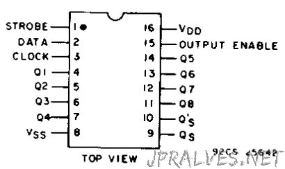
CD4094B is an 8-stage serial shift register having a storage latch associated with each stage for strobing data from the serial input to parallel buffered 3-state outputs. The parallel outputs may be connected directly to common bus lines. Data is shifted on positive clock transitions. The data in each shift register stage is transferred to the storage register when the STROBE input is high. Data in the storage register appears at the outputs whenever the OUTPUT-ENABLE signal is high.
Two serial outputs are available for cascading a number of CD4094B devices. Data is available at the QS serial output terminal on positive clock edges to allow for high-speed operation in cascaded systems in which the clock rise time is fast. The same serial information, available at the Q’Sterminal on the next negative clock edge, provides a means for cascading CD4094B devices when the clock rise time is slow.
The CD4094B types are supplied in 16-lead hermetic dual-in-line ceramic packages (F3A suffix), 16-lead dual-in-line plastic packages (E suffix), 16-lead small-outline packages (NSR suffix), and 16-lead thin shrink small-outline packages (PW and PWR suffixes).
Features
- 3-state parallel outputs for connection to common bus
- Separate serial outputs synchronous to both positive and negative clock edges for cascading
- Medium speed operation - 5 MHz at 10 V (typ.)
- Standardized, symmetrical output characteristics
- 100% tested for quiescent current at 20 V
- Maximum input current of 1 µA at 18 V over full package-temperature range; 100 nA at 18 V and 25°C
- Noise margin (full package temperature range):
- 1 V at VDD = 5 V
- 2 V at VDD = 10 V
- 2.5 V at VDD = 15 V
- 5-V, 10-V, and 15-V parametric ratings
- Meets all requirements of JEDEC Tentative Standard No. 13B, “Standard Specifications for Description of ‘B’ Series CMOS Devices”
Applications
- Serial-to-parallel data conversion
- Remote control holding register
- Dual-rank shift, hold, and bus applications
How to Build a Register Circuit with a 4094 Chip
(Link)
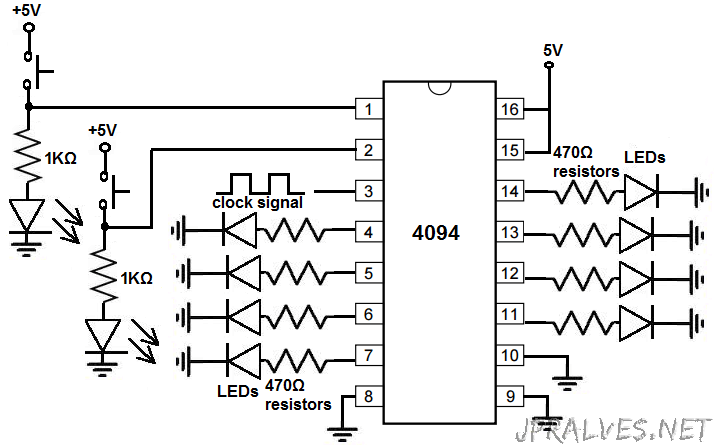
The 4094 works from voltage anywhere from 3V-15V. So we feed this voltage into VDD, pin 16 and we connect VSS to ground.
Pin 1 is the STROBE input. This input must be placed HIGH to transfer bits to the storage register. If this pin is LOW, no data can be transferred to the storage register so they won’t appear at the output.
Pin 2 is the data input. Depending on whether this pin is HIGH or LOW determines whether a 1 or 0 gets shifted into the register.
Pin 3 is the clock pin. The 4094 chip needs a clock signal in order to operate. Data gets shifted into the storage register on the rising edge of the clock signal.
Pin 15 is the Output Enable pin. This pin must be HIGH in order for the output pins to go HIGH. If this pin is LOW, outputs are disabled.
Pin 9 and 10, QS1 and QS2, are used for cascading a number of 4094 chips together. QS1 would be used to transfer data serial from one chip to the next on the positive edge of a clock signal with a clock that is high speed. QS2 would be used for transferring data serially from one chip to the other on the falling edge of a clock signal with a clock that is slow speed. So if you are cascading chips together, you either connect the QS1 or the QS2 pin to the data input pin of the second 4094 chip. This allows the shifting of data from one register chip to the next. Since we are not cascading multiple 4094s, we simply ground these pins.
QP0-QP7 are the output pins. To these pins, we attach our output device we want to turn on when a 1 is shifted to that pin.
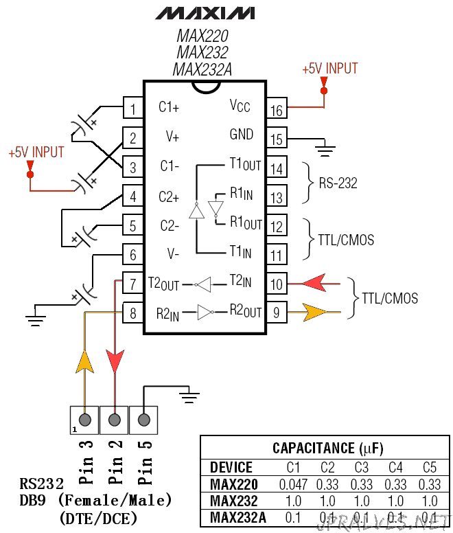
MAX232 - Dual EIA-232 Driver/Receiver
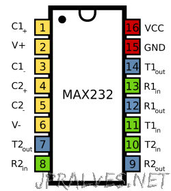
The MAX232 device is a dual driver/receiver that includes a capacitive voltage generator to supply TIA/EIA-232-F voltage levels from a single 5-V supply. Each receiver converts TIA/EIA-232-F inputs to 5-V TTL/CMOS levels. These receivers have a typical threshold of 1.3 V, a typical hysteresis of 0.5 V, and can accept ±30-V inputs. Each driver converts TTL/CMOS input levels into TIA/EIA-232-F levels.
Features
- Meets or Exceeds TIA/EIA-232-F and ITU Recommendation V.28
- Operates From a Single 5-V Power Supply With 1.0-µF Charge-Pump Capacitors
- Operates up to 120 kbit/s
- Two Drivers and Two Receivers
- ±30-V Input Levels
- Low Supply Current: 8 mA Typical
- ESD Protection Exceeds JESD 22
- 2000-V Human-Body Model (A114-A)
- Upgrade With Improved ESD (15-kV HBM) and 0.1-µF Charge-Pump Capacitors is Available With the MAX202 Device
Circuit: Serial Communication
(link)
LM2576 - SIMPLE SWITCHER® 40V, 3A Low Component Count Step-Down Regulator
The LM2576 series of regulators are monolithic integrated circuits that provide all the active functions for a step-down (buck) switching regulator, capable of driving 3A load with excellent line and load regulation. These devices are available in fixed output voltages of 3.3V, 5V, 12V, 15V, and an adjustable output version.
Requiring a minimum number of external components, these regulators are simple to use and include internal frequency compensation and a fixed-frequency oscillator.
The LM2576 series offers a high-efficiency replacement for popular three-terminal linear regulators. It substantially reduces the size of the heat sink, and in some cases no heat sink is required.
A standard series of inductors optimized for use with the LM2576 are available from several different manufacturers. This feature greatly simplifies the design of switch-mode power supplies.
Other features include a specified ±4% tolerance on output voltage within specified input voltages and output load conditions, and ±10% on the oscillator frequency. External shutdown is included, featuring 50 μA (typical) standby current. The output switch includes cycle-by-cycle current limiting, as well as thermal shutdown for full protection under fault conditions.
Features
- 3.3V, 5V, 12V, 15V, and Adjustable Output Versions
- Adjustable Version Output Voltage Range,1.23V to 37V (57V for HV Version) ±4% Max Over Line and Load Conditions
- Specified 3A Output Current
- Wide Input Voltage Range, 40V Up to 60V for HV Version
- Requires Only 4 External Components
- 52 kHz Fixed Frequency Internal Oscillator
- TTL Shutdown Capability, Low Power Standby Mode
- High Efficiency
- Uses Readily Available Standard Inductors
- Thermal Shutdown and Current Limit Protection
- P+ Product Enhancement Tested
Circuit

CD4022 - CMOS Octal Counter with 8 Decoded Outputs
CD4017B and CD4022B are 5-stage and 4-stage Johnson counters having 10 and 8 decoded outputs, respectively. Inputs include a CLOCK, a RESET, and a CLOCK INHIBIT signal. Schmitt trigger action in the CLOCK input circuit provides pulse shaping that allows unlimited clock input pulse rise and fall times.These counters are advanced one count at the positive clock signal transition if the CLOCK INHIBIT signal is low. Counter advancement via the clock line is inhibited when the CLOCK INHIBIT siganl is high. A high RESET signal clears the counter to its zero count. Use of the Johnson counter configuration permits high-speed operation, 2-input decode-gating and spike-free decoded outputs. Anti-lock gating is provided, thus assuring proper counting sequence. The decoded output are normally low and go high only at their respective decoded time slot. Each decoded output remains high for one full clock cycle. A CARRY-OUT signal completes on cycle every 10 clock input cycles in the CD4017B or every 8 clock input cycles in the CD4022B and is used to ripple-clock the succeeding device in a multi-device counting chain.The CD4017B and CD4022B types are supplied in 16-lead hermetic dual-in-line ceramic packages (F3A suffix), 16-lead dual-in-line plastic package (E suffix), 16-lead small-outline packages (NSR suffix), and 16-lead thin shrink small-outline packages (PW and PWR suffixes). The CD4017B types also are supplied in 16-lead small-outline packages (M and M96 suffixes).
Features
- Fully static operation
- Medium speed operation…10 MHz (typ.) at VDD = 10 V
- Standardized, symmetrical output characteristics
- 100% tested for quiescent current at 20 V
- 5-V, 10-V, and 15-V parametric ratings
- Meets all requirements of JEDEC Tentative Standard No. 13B, “Standard Specifications for Description of ’B’ Series CMOS Devices”
- Applications:
- Decade counter/decimal decode display (CD4017B)
- Binary counter/decoder
- Frequency division
- Counter control/timers
- Divde-by-N counting
- For further application information, see ICAN-6166 “COS/MOS MSI Counter and Register Design and Applications”
LM3914 - Dot/Bar Display Driver
The LM3914 is a monolithic integrated circuit that senses analog voltage levels and drives 10 LEDs, providing a linear analog display. A single pin changes the display from a moving dot to a bar graph. Current drive to the LEDs is regulated and programmable, eliminating the need for resistors. This feature is one that allows operation of the whole system from less than 3V.The circuit contains its own adjustable reference and accurate 10-step voltage divider. The low-bias-current input buffer accepts signals down to ground, or V−, yet needs no protection against inputs of 35V above or below ground. The buffer drives 10 individual comparators referenced to the precision divider. Indication non-linearity can thus be held typically to ½%, even over a wide temperature range.Versatility was designed into the LM3914 so that controller, visual alarm, and expanded scale functions are easily added on to the display system. The circuit can drive LEDs of many colors, or low-current incandescent lamps. Many LM3914s can be “chained” to form displays of 20 to over 100 segments. Both ends of the voltage divider are externally available so that 2 drivers can be made into a zero-center meter.The LM3914 is very easy to apply as an analog meter circuit. A 1.2V full-scale meter requires only 1 resistor and a single 3V to 15V supply in addition to the 10 display LEDs. If the 1 resistor is a pot, it becomes the LED brightness control. The simplified block diagram illustrates this extremely simple external circuitry.When in the dot mode, there is a small amount of overlap or “fade” (about 1 mV) between segments. This assures that at no time will all LEDs be “OFF”, and thus any ambiguous display is avoided. Various novel displays are possible.Much of the display flexibility derives from the fact that all outputs are individual, DC regulated currents. Various effects can be achieved by modulating these currents. The individual outputs can drive a transistor as well as a LED at the same time, so controller functions including “staging” control can be performed. The LM3914 can also act as a programmer, or sequencer.The LM3914 is rated for operation from 0°C to +70°C. The LM3914N-1 is available in an 18-lead PDIP (NFK) package.The following typical application illustrates adjusting of the reference to a desired value, and proper grounding for accurate operation, and avoiding oscillations.
Features
- Drives LEDs, LCDs or Vacuum Fluorescents
- Bar or Dot Display Mode Externally Selectable by User
- Expandable to Displays of 100 Steps
- Internal Voltage Reference from 1.2V to 12V
- Operates with Single Supply of Less than 3V
- Inputs Operate Down to Ground
- Output Current Programmable from 2 mA to 30 mA
- No Multiplex Switching or Interaction Between Outputs
- Input Withstands ±35V without Damage or False Outputs
- LED Driver Outputs are Current Regulated, Open-collectors
- Outputs can Interface with TTL or CMOS Logic
- The Internal 10-step Divider is Floating and can be Referenced to a Wide Range of Voltages
Circuit
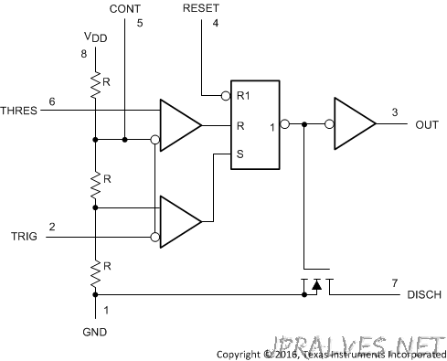
TLC555 - 2.1-MHz, 250-µA, Low-Power Timer
The TLC555 is a monolithic timing circuit fabricated using the TI LinCMOS™ process. The timer is fully compatible with CMOS, TTL, and MOS logic, and operates at frequencies up to 2 MHz. Because of its high input impedance, this device uses smaller timing capacitors than those used by the NE555. As a result, more accurate time delays and oscillations are possible. Power consumption is low across the full range of power-supply voltage. Like the NE555, the TLC555 has a trigger level equal to approximately one-third of the supply voltage and a threshold level equal to approximately two-thirds of the supply voltage. These levels can be altered by use of the control voltage terminal (CONT). When the trigger input (TRIG) falls below the trigger level, the flip-flop is set and the output goes high. If TRIG is above the trigger level and the threshold input (THRES) is above the threshold level, the flip-flop is reset and the output is low. The reset input (RESET) can override all other inputs and can be used to initiate a new timing cycle. If RESET is low, the flipflop is reset and the output is low. Whenever theoutput is low, a low-impedance path is provided between the discharge terminal (DISCH) and GND. All unused inputs must be tied to an appropriate logic level to prevent false triggering.
Features
- Very Low Power Consumption:
- 1 mW Typical at VDD = 5 V
- Capable of Operation in Astable Mode
- CMOS Output Capable of Swinging Rail to Rail
- High Output Current Capability
Circuit