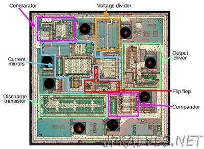
“This article explains how the LMC555 timer chip works, from the tiny transistors and resistors on the silicon chip, to the functional units such as comparators and current mirrors that make it work. The popular 555 timer integrated circuit is said to be the world’s best-selling integrated circuit with billions sold since it was designed in 1970 by analog IC wizard Hans Camenzind[1]. The LMC555 is a low-power CMOS version of the 555; instead of the bipolar transistors in the classic 555 (which I described earlier), the CMOS chip is built from low-power MOS transistors. The LMC555 chip can be understood by carefully examining the die photo.”
Related Content
Related Posts:
- Silicon die teardown: a look inside an early 555 timer chip
- 555 timer teardown: inside the world’s most popular IC
- Talking to memory: Inside the Intel 8088 processor’s bus interface state machine
- Inside an unusual 7400-series chip implemented with a gate array
- The Intel 8088 processor’s instruction prefetch circuitry: a look inside
- Reverse engineering standard cell logic in the Intel 386 processor
- Inside the Intel 386 processor die: the clock circuit
- Reverse engineering the Intel 386 processor’s register cell
- Examining the silicon dies of the Intel 386 processor
- How flip-flops are implemented in the Intel 8086 processor