
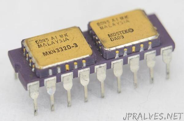
“In 1978, a memory chip stored just 16 kilobits of data. To make a 32-kilobit memory chip, Mostek came up with the idea of putting two 16K chips onto a carrier the size of a standard integrated circuit, creating the first memory module, the MK4332 “RAM-pak”. This module allowed computer manufacturers to double the density of their memory systems and by 1982, Mostek had sold over 3 million modules. The Apple III is the best-known system that used these memory modules.
This module was built from two 16-kilobit memory chips, constructed from the standard MK4116 dynamic RAM (DRAM) chip packaged in a leadless ceramic chip carrier; these are the golden rectangles on top of the carrier.
You might wonder why customers didn’t simply use these surface-mount packages directly, but at the time soldering surface-mount components was still a challenge for many customers. However, mounting two leadless chips on a dual inline-package (DIP) carrier allowed customers to double their memory density while still using their standard through-hole soldering techniques.
The purple carrier holding the chips was a ceramic substrate designed for thermal compatibility with the chips.1 There is no circuitry inside the ceramic carrier except wiring between the chips and the eighteen DIP pins. The two memory chips were wired in parallel except for their two select lines, which were kept separate. This allowed the desired memory chip to be selected. As a result, the MK4332 module has 18 pins, compared to 16 pins for the chips on top. Mostek used the same module design with the next generation of RAM chips, creating a 128-kilobit RAM module (MK4528) from two 64-kilobit RAM chips (MK4564).
Inside the 4116 memory chip
Although you might expect a complex mounting technique, the two 4116 chips are simply soldered onto the substrate with standard reflow techniques. For the photo below, I removed the metal lid from the left chip with a chisel and unsoldered the right chip with a hot air gun. On the left, you can see the rectangular silicon die inside the leadless carrier package. On the right are the 16 solder pads on the ceramic substrate. The wiring between the solder pads and the DIP pins is inside the ceramic substrate.”