
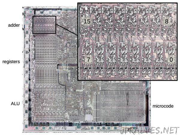
“The Intel 8086 processor contains many interesting components that can be understood through reverse engineering. In this article, I’ll discuss the adder that is used for address calculations. The photo below shows the tiny silicon die of the 8086 processor under a microscope. The left part of the chip has the 16-bit datapath including the registers and the Arithmetic-Logic Unit (ALU); you can see the pattern of circuitry repeated 16 times. The rectangle in the lower-right is the microcode ROM, defining the execution of each instruction.
The 16-bit adder, the topic of this post, is in the upper left. The magnified view shows how the adder is constructed from 16 stages, one for each bit. The upper row handles the top bits (15-8) and the lower row handles the low bits (7-0).1 Studying the die reveals how this 16-bit adder was optimized through clever circuit design, specialized logic gates, and careful layout techniques.
How the adder is used in the 8086
You might wonder why the 8086 contains both an adder and an ALU (arithmetic-logic unit). The reason is that the adder is used for address calculations, while the ALU is used for data calculations. The 8086 prefetches instructions using a “Bus Interface Unit”, which runs semi-independently from the “Execution Unit” that executed instructions. It would have been difficult for the Bus Interface Unit and the Execution Unit to share the ALU without conflicts. By providing both an adder2 and the ALU, the two calculations can take place in parallel.
Microprocessors of the early 1970s typically had 16-bit addresses, capable of accessing 64 kilobytes of memory. At first, 64 kilobytes seemed like more memory than anyone would need (or afford), but as the price of memory chips plunged, the demand for memory grew.4 To support a larger address space, Intel added segment registers to the 8086, a hack that allowed the processor to access a megabyte of memory but led to years of gnashed teeth. The concept is to break memory into 64-kilobyte segments. A segment register specifies the start of the memory segment, and a 16-bit address indicates an address within that segment. These are combined in the adder, as shown below, to obtain the memory address. One downside is that accessing regions of memory larger than 64 kilobytes is difficult; the segment register must be modified to get outside the current segment.”