
“Introduced in 1978, the revolutionary Intel 8086 microprocessor led to the x86 processors used in most desktop and server computing today. This chip is built from digital circuits, as you would expect. However, it also has analog circuits: charge pumps that turn the 8086’s 5-volt supply into a negative voltage to improve performance.1 I’ve been reverse-engineering the 8086 from die photos, and in this post I discuss the construction of these charge pumps and how they work.
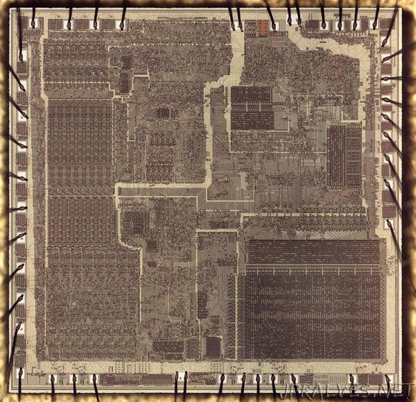
The photo above shows the tiny silicon die of the 8086 processor under a microscope. The metal layer on top of the chip is visible, with the silicon hidden underneath. Around the outside edge, bond wires connect pads on the die to the chip’s 40 external pins. However, careful examination shows that the die has 42 bond pads, not 40. Why are there two extra ones?
An integrated circuit starts with a silicon substrate, and transistors are built on this. For high-performance integrated circuits, it is beneficial to apply a negative “bias” voltage to the substrate. 2 To obtain this substrate bias voltage, many chips in the 1970s had an external pin that was connected to -5V,3 but this additional power supply was inconvenient for the engineers using these chips. By the end of the 1970s, however, on-chip “charge pump” circuits were designed that generated the negative voltage internally. These chips used a single convenient +5V supply, making engineers happier.”