
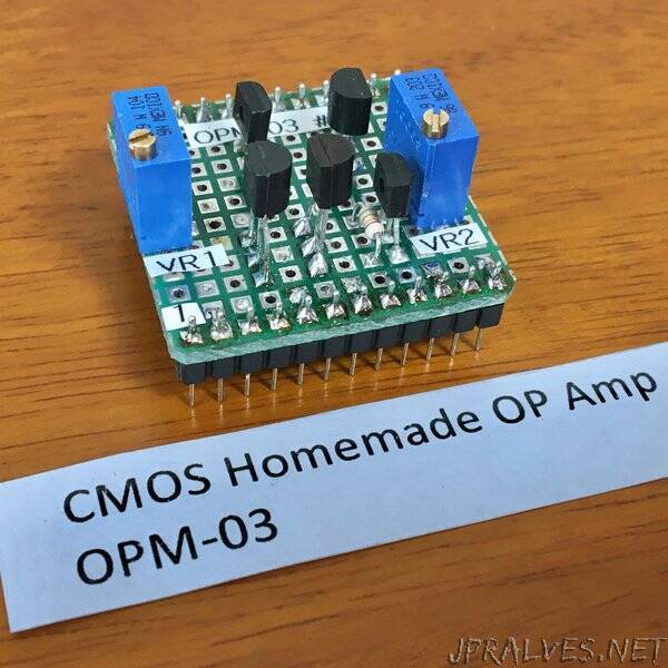
“CMOS Homemade Operational Amplifier module and a photo detector using it.
Operational amplifiers using the CMOS process are now widely used because of their low power consumption. Since the insulated gate of MOSFETs in the CMOS op-amps serves as the signal input, their input resistance is extremely large compared to operational amplifiers using bipolar transistors, and their bias current is extremely low. This time, I will explain how I boldly simplified its internal structure and built my own CMOS op-amp module using discrete MOSFETs to deepen my own understanding of its internal operating behavior and applications. I will also present an example of a self-made evaluation unit that allows experimentation with a non-inverting amplifier circuit, and a photo-detector circuit using a transimpedance amplifier.
1-1. Configuration of the CMOS simple discrete operational amplifier
In a previous my project, an experimental op-amp module with five bipolar transistors was introduced, and a similar configuration structure with five MOSFETs is used for this CMOS operational amplifier OPM-03. Because of the limited variety of single MOSFETs available and the fairly large variation in Vth, I thought it would be difficult to bring each internal part to an operating point that would allow overall operation, even if more FETs were used to improve the characteristics. Therefore, in this homemade project, it was decided that even if the characteristics were inferior to those of commercially available monolithic ICs, it would be sufficient if I could manage to achieve operation as a CMOS operational amplifier and experience its features.
1-2. Differential pair
As shown in Fig. 1, the differential pair consists of TR1 and TR2 N-Channel MOSFETs. The load of the differential pair is the resistors R1 and R2. Typically, a current mirror is used for this load; VR1 and R7 are substitutes for the bias and current sources of a typical differential pair. The drain DC potential of TR1 must be such that the gate potential of the second stage TR3 is operational and the DC offset of the third stage output is zero. It is this VR1 that sets the differential pair operating points so that the drain potential of TR1 satisfies these conditions.
1-3. Gain stage
The gain stage consists only of TR3, a P-Channel MOSFET; C1 is a phase compensation capacitor to prevent parasitic oscillation.VR2, R6 and R3 are the loads of TR3. The potential difference created by VR2 and R6 is to provide a difference in the gate potential of the third stage source follower to eliminate crossover distortion.
1-4. Source follower
The third stage is a complementary source follower with N-channel MOSFET TR4 and P-channel MOSFET TR5. R4 and R5 are simple protection resistors to limit excessive drain current of TR4 or TR5 in case of output short circuit. However, the power rating of these resistors should be about 2 W. The small resistors pictured in Fig. 3 are not correct.
1-5. Evaluation unit
Figure 4 shows the circuit diagram of the evaluation unit for the homemade discrete operational amplifier module. The non-inverting amplifier circuit, open-loop operation, and photo detector operation with transimpedance amplifier configuration are made possible by toggle switches. The gain can be switched with a rotary switch. Figure 5 shows the inside of this evaluation unit.”