
“A completely redesigned MCP23017 IO expander breakout, easy to use and breadboard friendly.
New style MCP23017 Breakout – Top view
There will not be a lot of obvious differences at first, but if we look closely, here are the changes:– In the old version, due to the size of the SOIC28 footprint, I had to place the bypass capacitors, as well as I2C pullup resistors on the bottom layer of the PCB.
- The new design, using the more readily available ( at least where I live) SSOP28 footprint, leaves enough space for these components on the top layer, thus resulting in a mostly single-layer layout, with only a few tracks on the bottom layer.
- I2C pull-up resistors can now be controlled by a jumper, enabling or disabling them completely… This helps when adding a few devices to the I2C bus, and rather having the pull-up’s close to the MCU ( as is generally recommended anyway )
- Other cosmetic changes involve the separation of the data ports (A and B) from the interrupts, reset, Vcc and ground pins. On initial testing of this on a breadboard, it makes using the device a bit easier, and access to the io pins faster. ( In my biased opinion anyway )
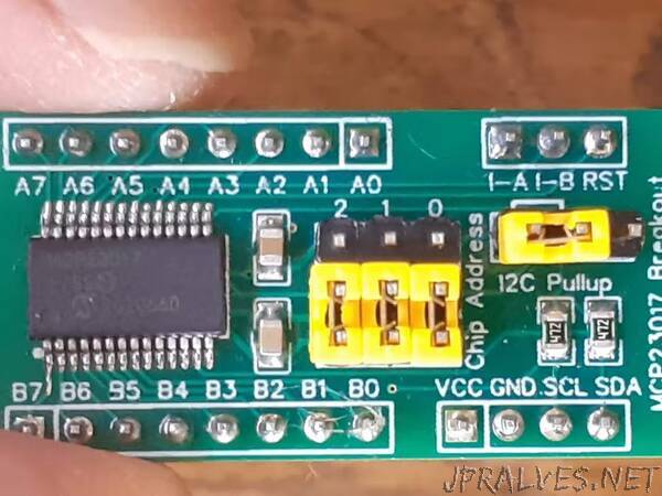
Pinouts and connections
I have tried to make all the connections easy to find and use, with the IO ports ( A and B) on opposite sides of the breakout, Numbered A7 to A0 on the top, and B7 to B0 on the bottom. VCC, GND, SCL and SDA are on a separate 4-way header pin, with the two interrupt pins (I-A and I-B) together with the reset (RST) pin on a 3-way header opposite the power and signal header..
Addressing pins are in the centre of the PCB, marked with a 2 1 0 ( for AD2, AD1, and AD0 respectively), Jumpers to the bottom ( towards port B) pull the pins to ground, where the opposite side will pull the address pins high. To the right of that, another 3-way jumper enables or disables the I2C pull-resistors on the module, which in this case is set at 4k7.”