
“Continuing with my simple FIR filter Verilog module, this project walks through how to rewrite HDL logic when setup timing violations occur.
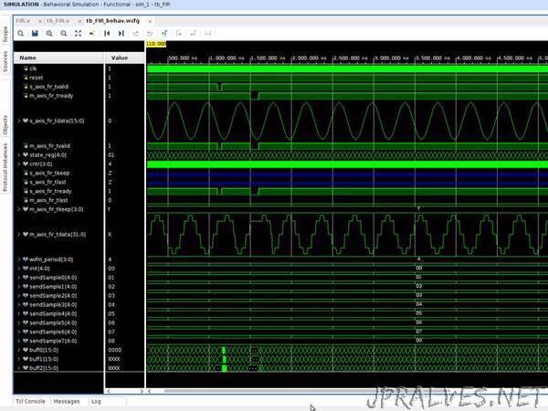
In my last project, I demonstrated the initial steps to writing a custom FIR module in Verilog. That project resulted in a LPF FIR that functioned properly in the behavioral simulation, but failed to meet timing requirements when placed and routed into a design.
Starting with the design as is from the previous project, let’s walk though how to analyze a design when it fails to meet timing requirements. Timing requirements are first determined in the implementation of a design in Vivado when the logic is being placed and routed in the fabric of the target FPGA chip (in this case it is the Zynq 7020 on the Arty Z7 development board that I’m using).
I chose to import the FIR as an RTL module into a block design for the Arty Z7 where a DDS compiler being streamed phase increment offset values from memory via an AXI DMA (direct memory access) block can input varying frequency sinusoids to demonstrate how the LPF FIR behaves.”