
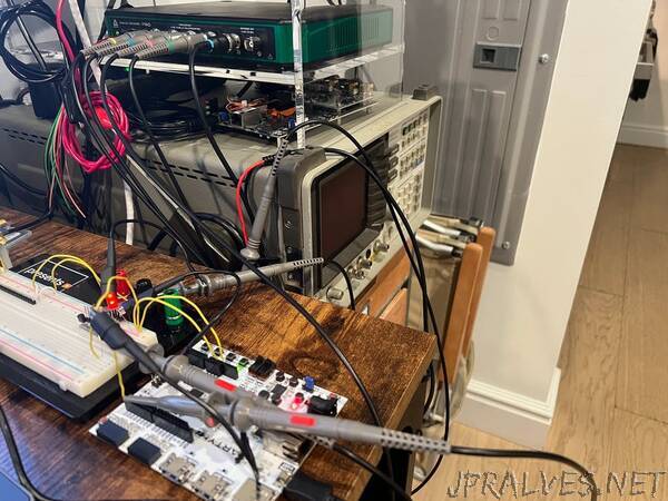
“Using the ADP3450, this project measures amount of delay between asserting FPGA IO on base of NPN 2N3094 and LED illuminating on collector.
Signal timing is a huge component in FPGA design, and while many tutorials demonstrate how to handle timing within the programmable logic I thought it would be helpful to show how to measure external circuitry timing when it’s being driven by an FPGA’s I/O and has a direct impact on the timing of the logic in RTL.
Recently I posted a project about driving a 5-digit 7-segment display with an FPGA where I had to calculate the proper refresh rate of how long a character needed to be held on each display to appear stable to the human eye. Each common cathode of the 5 7-segment displays where connected to the collector of an NPN 2N3904 BJT that were connected to ground by an I/O pin from the FPGA being set high. Thus, past of this timing of the overall refresh rate included how long it would take for the collector to be connected to the emitter (and ultimately ground) after the FPGA I/O signal was asserted.
Using the oscilloscope function of my Analog Discovery Pro ADP3450 with its control interface software WaveForms, I set up a test circuit with a single 2N3904 and LED on its collector to measure the amount of delay between the FPGA I/O pin being asserted on the base of the BJT to when the LED is illuminated. Which effectively is measuring the slew of the BJT to add as an offset value to the refresh rate in the RTL logic driving the scrolling text across the 5-digit 7-segment display.
Overall, each character on needs to be held on the 7-segment display for 1 millisecond plus the slew of the 2N3904 BJT.”