
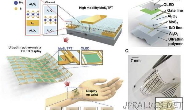
“A team of researchers from Yonsei University, and Chung-Ang University, both in Korea, has developed a MoS2 transistor that can be used with bendable OLED displays. In their paper published on the open access site Science Advances, the group explains overcoming the problem of resistance between the MoS2 and a transistor’s source and drain to create an operational bendable 6x6 pixel array.
As phone makers seek ways to separate themselves from their competitors, research continues into the idea of a truly bendable product, which would include a bendable screen. There have been advances, but to date, there is still not a commercially available phone that can be bent like a piece of paper and shoved in a back pocket. In this new effort, the researchers report that they have overcome one of the hurdles involved in bringing a truly bendable phone, television or other screen device to market.
One of the serious roadblocks to bendable devices is the resistance that occurs between MoS2 and a transistor’s source and drain electrodes—it is just too high for practical use. To overcome this problem, the researchers placed the transistor between two layers of aluminum oxide instead of on a piece of silicon dioxide as has been traditionally done. They note that the interface between the two materials enhanced the flow of electrons into the semiconductor, which served to overcome the resistance encountered with other approaches. The result, they add, was a boost in charge carrier mobility. They note also that because of its smoothness, there were no places where charge could become trapped, which, they claim, improved mobility even more.
The researchers demonstrated their idea by creating a 6x6 pixel-array display device that could be affixed to the skin like a Band-Aid—it was capable of displaying numbers, like an old-fashioned calculator. The team reports that the bendable device (which was just seven micrometers thick) could withstand bending to a radius of one millimeter repeatedly.
More research is required to find out if the technique can be scaled for use in a high-resolution device, and if so, if it can be done in an economical way.”