
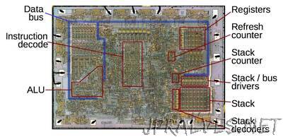
“The revolutionary Intel 8008 microprocessor is 45 years old today (March 13, 2017), so I figured it’s time for a blog post on reverse-engineering its internal circuits. One of the interesting things about old computers is how they implemented things in unexpected ways, and the 8008 is no exception. Compared to modern architectures, one unusual feature of the 8008 is it had an on-chip stack for subroutine calls, rather than storing the stack in RAM. And instead of using normal binary counters for the stack, the 8008 saved a few gates by using shift-register counters that generated pseudo-random values. In this article, I reverse-engineer these circuits from die photos and explain how they work. The image below shows the 8008’s tiny silicon die, highly magnified. Around the outside of the die, you can see the 18 wires connecting the die to the chip’s external pins. The 8008’s circuitry is built from about 3500 tiny transistors (yellow) connected by a metal wiring layer (white). This article will focus on the stack circuits on the right side of the chip and how they interact with the data bus (blue).”