
“Artificial intelligence (AI) plays an important role in many systems, from predictive text to medical diagnoses. Inspired by the human brain, many AI systems are implemented based on artificial neural networks, where electrical equivalents of biological neurons are interconnected, trained with a set of known data, such as images, and then used to recognize or classify new data points.
In traditional neural networks used for image recognition, the image of the target object is first formed on an image sensor, such as the digital camera in a smart phone. Then, the image sensor converts light into electrical signals, and ultimately into the binary data, which can then be processed, analyzed, stored and classified using computer chips. Speeding up these abilities is key to improving any number of applications, such as face recognition, automatically detecting text in photos, or helping self-driving cars recognize obstacles.
While current, consumer-grade image classification technology on a digital chip can perform billions of computations per second, making it fast enough for most applications, more sophisticated image classification such as identifying moving objects, 3D object identification, or classification of microscopic cells in the body, are pushing the computational limits of even the most powerful technology. The current speed limit of these technologies is set by the clock-based schedule of computation steps in a computer processor, where computations occur one after another on a linear schedule.
To address this limitation, Penn Engineers have created the first scalable chip that classifies and recognizes images almost instantaneously. Firooz Aflatouni, Associate Professor in Electrical and Systems Engineering, along with postdoctoral fellow Farshid Ashtiani and graduate student Alexander J. Geers, have removed the four main time-consuming culprits in the traditional computer chip: the conversion of optical to electrical signals, the need for converting the input data to binary format, a large memory module, and clock-based computations.
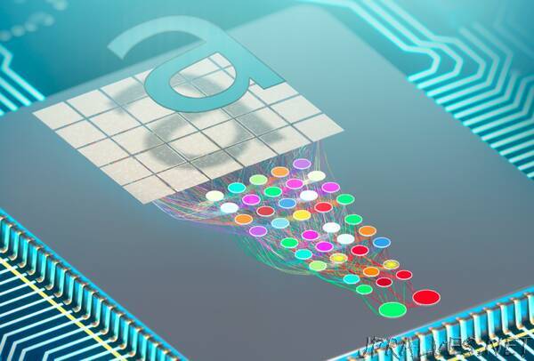
They have achieved this through direct processing of light received from the object of interest using an optical deep neural network implemented on a 9.3 square millimeter chip.
The study, published in Nature, describes how the chip’s many optical neurons are interconnected using optical wires or “waveguides” to form a deep network of many “neuron layers” mimicking that of the human brain. Information passes through the layers of the network, with each step helping to classify the input image into one of its learned categories. In the researchers’ study, the images the chip classified were of hand-drawn, letter-like characters.
Just like the neural network in our brains, this deep network is designed in a way that allows for rapid information processing. The researchers demonstrated that their chip can perform an entire image classification in half of a nanosecond — the time it takes traditional digital computer chips to complete just one computation step on their clock-based schedule.
“Our chip processes information through what we call ‘computation-by-propagation,’ meaning that unlike clock-based systems, computations occur as light propagates through the chip,” says Aflatouni. “We are also skipping the step of converting optical signals to electrical signals because our chip can read and process optical signals directly, and both of these changes make our chip a significantly faster technology.”
The chip’s ability to process optical signals directly lends itself to another benefit.
“When current computer chips process electrical signals they often run them through a Graphics Processing Unit, or GPU, which takes up space and energy,” says Ashtiani. “Our chip does not need to store the information, eliminating the need for a large memory unit.”
“And, by eliminating the memory unit that stores images, we are also increasing data privacy,” Aflatouni says. “With chips that read image data directly, there is no need for photo storage and thus, a data leak does not occur.”
A chip that reads information at light speed and provides a higher degree of cybersecurity would undoubtedly have an impact in many fields; this is one of the reasons research into this technology has ramped up in the past several years.
“We aren’t the first to come up with technology that reads optical signals directly,” says Geers, “but we are the first to create the complete system within a chip that is both compatible with existing technology and scalable to work with more complex data.”
The chip, with its deep network design, requires training to learn and classify new data sets, similar to how humans learn. When presented with a given data set, the deep network takes in the information and classifies it into previously learned categories. This training needs to strike a balance that is specific enough to result in accurate image classifications and general enough to be useful when presented with new data sets. The engineers can “scale up” the deep network by adding more neural layers, allowing the chip to read data in more complex images with higher resolution.
And, while this new chip will advance current image sensing technology, it can be used for countless applications across a variety of data types.
“What’s really interesting about this technology is that it can do so much more than classify images,” says Aflatouni. “We already know how to convert many data types into the electrical domain – images, audio, speech, and many other data types. Now, we can convert different data types into the optical domain and have them processed almost instantaneously using this technology.”
But what does it look like when information is processed at the speed of light?
“To understand just how fast this chip can process information, think of a typical frame rate for movies,” he continues. “A movie usually plays between 24 and 120 frames per second. This chip will be able to process nearly 2 billion frames per second! For problems that require light speed computations, we now have a solution, but many of the applications may not be fathomable right now.”
With a piece of technology that has many applications, it is important to understand its abilities and limitations at more fundamental levels, and Aflatouni’s current and future plans for this research will do just that.
“Our next steps in this research will examine the scalability of the chip as well as work on three-dimensional object classification,” says Aflatouni. “Then maybe we will venture into the realm of classifying non-optical data. While image classification is one of the first areas of research for this chip, I am excited to see how it will be used, perhaps together with digital platforms, to accelerate different types of computations.””