
“Advances in microelectronics – also known as microchips or chips – have enabled fast, powerful, compact smartphones and laptops – electronic devices that were once, long ago, the stuff of science fiction.
Chips consist of miniaturized components called transistors – tiny silicon switches that process and store data as ones and zeroes, the binary language of computers. The more transistors a chip has, the faster it can process data. The most sophisticated chip today is about the size of a fingernail and consists of more than 100 billion transistors.
Since the 1960s, the chip industry has relied on lithography – a technique that uses light to print tiny patterns on silicon to mass produce microchips. Through the decades, advances in lithography have enabled the use of smaller and smaller wavelengths and thus fabricate smaller transistors. During the early years of chip innovation, lithography tools once used visible light, with wavelengths as small as 400 nanometers (nm), and then ultraviolet light (as small as 248 nm) and deep ultraviolet light (193 nm).
Today, the chip industry has entered a new era: extreme ultraviolet lithography (EUVL), a revolutionary technique that deploys short wavelengths of just 13.5 nanometers, which is about 40 times smaller than visible light and 20 times smaller than UV light. Such a short EUV wavelength allows the microelectronics industry to print microchip circuits and transistors that are tens of thousands of times thinner than a strand of human hair – and buy more time for Moore’s Law, which predicted in 1965 that the number of transistors placed on a chip would double every two years until the technology reached its limitations in miniaturization and performance.
“When you’re talking about the future of semiconductor manufacturing, we’re talking about extending Moore’s Law – and that has been our primary focus for decades,” says Patrick Naulleau, a leading expert in the complex science behind EUVL and the director of the Center for X-Ray Optics, a research facility located at the Department of Energy’s Lawrence Berkeley National Laboratory (Berkeley Lab).
EUV lithography was recently commercialized in 2019, but it took decades of research to get there, much of which was made possible by the unique capabilities of the CXRO. For the past 25 years, CXRO scientists and engineers have worked side by side with microelectronics industry leaders to tackle the significant technological advances required to develop EUVL.
According to Naulleau, the tiny wavelength in EUVL is very close to X-ray light and therefore requires new instruments that far exceed the capabilities of early lithography, which employed longer and less energetic wavelengths of visible and ultraviolet light. (On the electromagnetic spectrum, a system scientists use to classify all ranges of light according to their corresponding wavelength, X-ray light ranges from 0.01 to 10 nanometers; extreme ultraviolet or EUV light ranges from 10 to 124 nanometers; and UV light from 124 to 400 nanometers, Naulleau explains.)
Some analysts say that the end of Moore’s Law is near. But it could be decades before the modern chip runs out of room for improvement, thanks to advances in materials and instrumentation enabled by the CXRO, Naulleau says.
He shares his perspective in this Q&A.
Q: How has CXRO helped drive innovation in chip making?
The CXRO has helped industry understand the fundamental science behind EUVL, and how to push the technology forward.
In 1997, Intel, IBM, AMD, and Motorola formed the EUV LLC consortium to fund work at three national labs – Berkeley Lab, Livermore Lab, and Sandia – to develop the world’s first EUV lithography scanner for the semiconductor industry. I had just completed my Ph.D. when I was recruited by CXRO to work on the project. I’m proud to say that our work helped lay the foundation for the full commercialization of EUV lithography, which finally happened in 2019.
In 2001, as EUV lithography gained more traction across the industry as a whole, we kicked off a partnership with SEMATECH, which was a broad-based semiconductor industry consortium, to continue pushing EUV lithography research forward.
Despite the successful commercial launch of EUV lithography in 2019, there’s still more basic science work to be done to keep the technology moving forward – and we continue to partner with Intel, Samsung, and other industry leaders in the drive to develop future EUV lithography systems capable of printing ever smaller, faster, and more energy-efficient chips.
Q: How is EUV lithography used to make microchips?
Naulleau: First, a photoresist is spread on top of a silicon wafer. A photoresist is a light-sensitive chemical film like we used to use in old-school film cameras.
Then, a sophisticated camera called a lithography tool projects images of tiny circuits onto the photoresist-coated wafer using EUV light at a wavelength of 13.5 nanometers. The photoresist captures the ultrahigh resolution image of the computer chip circuits.
Basically, you can think of the lithography tool as a very fancy photocopier for computer chips.
After the images of the circuits are recorded in the photoresist film, etching tools are used to transfer those circuit patterns into the silicon wafer, eventually forming hundreds of computer chips on each 12-inch wafer.
Q: What is the CXRO doing now to push chip innovation forward?
During the pandemic, we continued to partner with Intel and Samsung to push the capabilities of our next generation EUV lithography research tools and to develop new chemical analysis tools that allow us to understand the fundamental physics of how photoresists work.
Right now, our latest lithography tools are able to produce features that are smaller than can be reliably recorded in the photoresist, so the most immediate challenge the industry is facing is in the understanding and development of new photoresist materials that will enable fabrication of chips at the 14-angstrom node (1.4 nanometers) and below. (1 angstrom is 10 million times smaller than a millimeter – or the approximate size of a single hydrogen atom.)
That’s our value add – we do the fundamental research needed to accelerate technology a decade ahead of the game because the microchip industry doesn’t have time to wait.
Q: How does the CXRO produce EUV light?
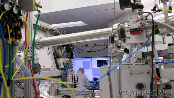
For the past 25 years, CXRO’s EUVL instruments have harnessed light from Berkeley Lab’s Advanced Light Source, a synchrotron user facility that produces very bright extreme ultraviolet and soft X-ray light that’s guided down highly specialized instruments called “beamlines” to experiment stations.
We’re one of the first DOE labs to develop the basic research for EUVL systems – so industry relies on us to develop new EUV research and development instrumentation such as advanced microfield lithography and microscopy tools.”