
“Solar panels, cameras, biosensors and fiber optics are technologies that rely on photodetectors, or sensors that convert light into electricity. Photodetectors are becoming more efficient and affordable, with their component semiconductor chips decreasing in size. However, this miniaturization is pushing against limits set by current materials and manufacturing methods, forcing trade-offs between size and performance.
There are many limitations of the traditional semiconductor chip manufacturing process. The chips are created by growing the semiconductor film over the top of a wafer in a way where the film’s crystalline structure is in alignment with that of the substrate wafer. This makes it difficult to transfer the film to other substrate materials, reducing its applicability.
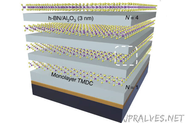
The current method of transferring and stacking these films is done through mechanical exfoliation, a process where a piece of tape pulls off the semiconductor film and then transfers it to a new substrate, layer by layer. This process results in multiple nonuniform layers stacked upon one another with each layer’s imperfections accumulated in the whole.
Certain materials do not function well as extremely thin layers. Silicon remains ubiquitous as the material of choice for semiconductor chips, however, the thinner it gets, the worse it performs as a photonic structure, making it less than ideal in photodetectors.
Manufacturing uniform, extremely thin, high quality photonic semiconductor films of material other than silicon would make semiconductor chips more efficient, applicable, and scalable.
Penn Engineers Deep Jariwala, assistant professor in electrical and systems engineering, and Pawan Kumar and Jason Lynch, a postdoctoral fellow and a doctoral student in his lab, led a study published in Nature Nanotechnology that aims to do just that. Eric Stach, professor in materials science and engineering, along with his postdoc Surendra Anantharaman, doctoral student Huiqin Zhang and undergraduate student Francisco Barrera also contributed to this work.
The team grew monolayers of atoms, or lattices, on a two-inch wafer and then dissolved the substrate, which allows the lattice to be transferred to any desired material, in their case, sapphire. Additionally, their lattice was created with repeating units of atoms aligned in one direction to make the superlattice two-dimensional, compact and efficient. Their superlattice design is not only extremely thin, making it lightweight and cost effective, it can also emit light, not just detect it.”