
“The Big Data revolution has strained the capabilities of state-of-the-art electronic hardware, challenging engineers to rethink almost every aspect of the microchip. With ever more enormous data sets to store, search and analyze at increasing levels of complexity, these devices must become smaller, faster and more energy efficient to keep up with the pace of data innovation.
Ferroelectric field effect transistors (FE-FETs) are among the most intriguing answers to this challenge. Like traditional silicon-based transistors, FE-FETs are switches, turning on and off at incredible speed to communicate the 1s and 0s computers use to perform their operations.
But FE-FETs have an additional function that conventional transistors do not: their ferroelectric properties allow them to hold on to electrical charge.
This property allows them to serve as non-volatile memory devices as well as computing devices. Able to both store and process data, FE-FETs are the subject of a wide range of research and development projects. A successful FE-FET design would dramatically undercut the size and energy usage thresholds of traditional devices, as well as increase speed.
Researchers at the University of Pennsylvania School of Engineering and Applied Science have introduced a new FE-FET design that demonstrates record-breaking performances in both computing and memory.
A recent study published in Nature Nanotechnology led by Deep Jariwala, Associate Professor in the Department of Electrical and Systems Engineering (ESE), and Kwan-Ho Kim, a Ph.D. candidate in his lab, debuted the design. They collaborated with fellow Penn Engineering faculty members Troy Olsson, also Associate Professor in ESE, and Eric Stach, Robert D. Bent Professor of Engineering in the Department of Materials Science and Engineering (MSE) and Director of the Laboratory for Research on the Structure of Matter (LRSM).
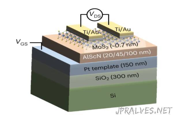
The transistor layers a two-dimensional semiconductor called molybdenum disulfide (MoS2) on top of a ferroelectric material called aluminum scandium nitride (AlScN), demonstrating for the first time that these two materials can be effectively combined to create transistors at scales attractive to industrial manufacturing.
“Because we have made these devices combining a ferroelectric insulator material with a 2D semiconductor, both are very energy efficient,” says Jariwala. “You can use them for computing as well as memory — interchangeably and with high efficiency.”
The Penn Engineering team’s device is notable for its unprecedented thinness, allowing for each individual device to operate with a minimum amount of surface area. In addition, the tiny devices can be manufactured in large arrays scalable to industrial platforms.
“With our semiconductor, MoS2, at a mere 0.7 nanometers, we weren’t sure it could survive the amount of charge that our ferroelectric material, AlScN, would inject into it,” says Kim. “To our surprise, not only did both of them survive, but the amount of current this enables the semiconductor to carry was also record-breaking.”
The more current a device can carry, the faster it can operate for computing applications. The lower the resistance, the faster the access speed for memory.
This MoS2 and AlScN combination is a true breakthrough in transistor technology. Other research teams’ FE-FETs have been consistently stymied by a loss of ferroelectric properties as devices miniaturize to approach industry-appropriate scales.
Until this study, miniaturizing FE-FETs has resulted in severe shrinking of the “memory window.” This means that as engineers reduce the size of the transistor design, the device develops an unreliable memory, mistaking 1s for 0s and vice versa, compromising its overall performance.
The Jariwala lab and collaborators achieved a design that keeps the memory window large with impressively small device dimensions. With AlScN at 20 nanometers, and MoS2 at 0.7 nanometers, the FE-FET dependably stores data for quick access.
“The key,” says Olsson, “is our ferroelectric material, AlScN. Unlike many ferroelectric materials, it maintains its unique properties even when very thin. In a recent paper from my group, we showed that it can we can retain its unique ferroelectric properties at even smaller thicknesses: 5 nanometers.”
The Penn Engineering team’s next steps are focused on this further miniaturization to produce devices that operate with voltages low enough to be compatible with leading-edge consumer device manufacturing.
“Our FE-FETs are incredibly promising,” says Jariwala. “With further development, these versatile devices could have a place in almost any technology you can think of, especially those that are AI-enabled and consume, generate or process vast amounts of data — from sensing to communications and more.”“