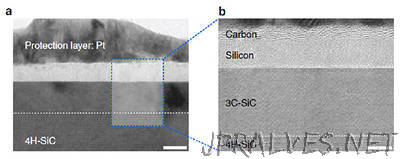
“All our smart phones have shiny flat AMOLED displays. Behind each single pixel of these displays hide at least two silicon transistors which were mass-manufactured using laser annealing technologies. While the traditional methods to make them uses temperatures above 1,000°C, the laser technique reaches the same results at low temperatures even on plastic substrates (melting temperature below 300°C). Interestingly, a similar procedure can be used to generate crystals of graphene. Graphene is a strong and thin nano-material made of carbon, its electric and heat-conductive properties have attracted the attention of scientists worldwide. Prof. KEON Jae Lee’s research group at the Center for Multidimensional Carbon Materials within the Institute for Basic Science (IBS) and Prof. CHOI Sung-Yool’s team at KAIST discovered graphene synthesis mechanism using laser-induced solid-state phase separation of single-crystal silicon carbide (SiC). This study, available on Nature Communications, clarifies how this laser technology can separate a complex compound (SiC) into its ultrathin elements of carbon and silicon.”
