

Other
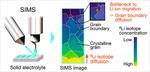
“A research team has developed a new technique to image grain boundaries obstructing lithium-ion migration in solid-state batteries — a promising type of next-generation battery. A NIMS research team has developed a new technique to image grain boundaries obstructing lithium-ion migration …
“NIMS and Osaka University Graduate School of Engineering have succeeded in fabricating a nickel single crystal with only a very few crystalline defects by irradiating nickel powder with a large-radius, flat-top laser beam (i.e., a laser beam whose intensity …

“NIMS and AIST developed a liquid electret material capable of semi-permanently retaining static electricity. They subsequently combined this material with soft electrodes to create the first bendable, stretchable vibration-powered device in the world. Because this device is highly deformable and …
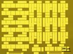
“NIMS succeeded in fabricating topological LC circuits arranged in a honeycomb pattern where electromagnetic (EM) waves can propagate without backscattering even when pathways turn sharply. Engineers have succeeded in fabricating topological LC circuits arranged in a honeycomb pattern where electromagnetic …
“A NIMS-Ehime University joint research team succeeded in discovering new materials that exhibit superconductivity under high pressures using materials informatics (MI) approaches (data science-based material search techniques). This study experimentally demonstrated that MI enables efficient exploration of new superconducting …
“When power generators like windmills and solar panels transfer electricity to homes, businesses and the power grid, they lose almost 10 percent of the generated power. To address this problem, scientists are researching new diamond semiconductor circuits to make power …

“WPI-MANA has developed the world’s highest performance dielectric nanofilms using atomically thin perovskites. This technology may revolutionize the next-generation of electronics. This research was conducted by a WPI-MANA research group led by Principal Investigator Minoru Osada and …
“Just as magnets attract iron particles in sandpits, permanent magnetics only attract one type of ion in an electrochemical solution, constituting the basis of magnetically controlled electrochemical transistors. Electrochemical devices find application in many technologies, including batteries, capacitors, sensors, and …
“A NIMS research group has succeeded for the first time in the world in developing a logic circuit equipped with diamond-based MOSFETs (metal-oxide-semiconductor field-effect-transistors) at two different operation modes. This achievement is a first step toward the development of diamond …

“As consumers around the world have become increasingly dependent on electronics, the transistor, a semiconductor component central to the operation of these devices, has become a critical subject of scientific research. Over the last several decades, scientists and engineers have …