
“WPI-MANA has developed the world’s highest performance dielectric nanofilms using atomically thin perovskites. This technology may revolutionize the next-generation of electronics.
This research was conducted by a WPI-MANA research group led by Principal Investigator Minoru Osada and Director Takayoshi Sasaki of WPI-MANA at NIMS. Electronic devices are getting smaller all the time, but there is a limit to how small they can get using current materials and technology. High-κ dielectric materials may be the key for developing electronic devices of the future.
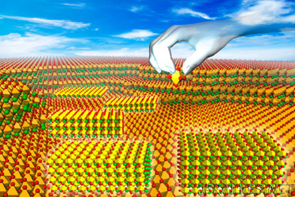
Minoru Osada and colleagues created high-performance dielectric nanofilms using 2D perovskite nanosheets (Ca2Nam−3NbmO3m+1; m = 3–6) as building blocks. Perovskite oxides offer tremendous potential for controlling their rich variety of electronic properties including high-κ dielectric and ferroelectric.
The researchers demonstrated the targeted synthesis of nanofilms composed of 2D perovskite nanosheets in a unit-cell-upon-unit-cell manner. In this unique system, perovskite nanosheets enable precise control over the thickness of the perovskite layers in increments of ~0.4 nm (one perovskite unit) by changing m, and such atomic layer engineering enhances the high-κ dielectric response and local ferroelectric instability. The m = 6 member (Ca2Na3Nb6O19) attained the highest dielectric constant, εr = ~470, ever realized in all known dielectrics in the ultrathin region of less than 10 nm.
Perovskite nanosheets are of technological importance for exploring high-κ dielectrics in 2D materials, which have great potential in electronic applications such as memories, capacitors, and gate devices. Notably, perovskite nanosheets afforded high capacitances by relying on high-κ values at a molecular thickness. Ca2Na3Nb6O19 exhibited an unprecedented capacitance density of approximately 203 μF cm-2, which is about three orders of magnitude greater than that of currently available ceramic condensers, opening a route to ultra-scaled high-density capacitors.
These results provide a strategy for achieving 2D high-κ dielectrics/ferroelectrics for use in ultra-scaled electronics and post-graphene technology.”