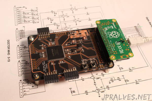
“What a Lattice iCE40 FPGA needs
A clock input. Has to be provided by an oscillator, it doesn’t have a crystal driver.
1.2v core supply for the internal logic.
2.5v non volatile memory supply. Can be provided via a voltage drop over a diode from 3.3v.
IO supply for the IO pins, different banks of IO can have different supplies. This design uses 3.3v for all banks.
Get configured over SPI interface. This can be done directly by a microcontroller or a computer, or the bitstream can be programmed into some FLASH, and the FPGA will read it at boot. If FLASH isn’t provided then the bitstream needs to be programmed at every power up or configuration reset.
Decoupling capacitors for each IO bank.”
