
“Enabling next-generation silicon designs targeting advanced mobile and high-performance computing applications
TSMC today announced delivery of the complete version of its 5 nanometer (nm) design infrastructure within the Open Innovation Platform® (OIP). This full release enables 5nm systems-on-chip (SoC) designs in next-generation advanced mobile and high-performance computing (HPC) applications, targeting high-growth 5G and artificial intelligence markets. Leading Electronic Design Automation (EDA) and IP vendors collaborated with TSMC to develop and validate the complete design infrastructure, including technology files, process design kits (PDKs), tools, flows and IP, through multiple silicon test vehicles.
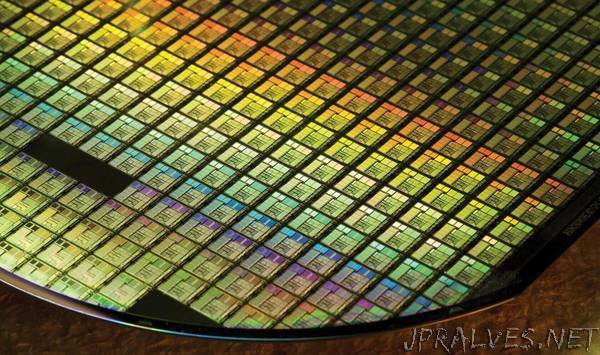
TSMC’s 5nm process is already in risk production and offers IC designers a new level of performance and power optimization targeted at the next generation of high-end mobile and HPC applications. Compared with TSMC’s 7nm process, its innovative scaling features deliver 1.8X logic density and 15% speed gain on an ARM® Cortex®-A72 core, along with superior SRAM and analog area reduction enabled by the process architecture. The 5nm process enjoys the benefits of process simplification provided by EUV lithography, and is making excellent progress in yield learning, achieving the best technology maturity at the same corresponding stage as compared to TSMC’s previous nodes.
TSMC’s comprehensive 5nm design infrastructure includes the full versions of the 5nm Design Rule Manual (DRM), SPICE model, process design kits (PDKs) and silicon-validated foundation and interface IP, and also supports a full range of certified EDA tools and design flows. Backed by the resources of the largest design ecosystem in the industry, TSMC’s Open Innovation Platform®, customers have already started intensive design engagements, paving the way for product tape-outs, pilot activities and early sampling.
“TSMC’s 5-nanometer technology offers our customers the industry’s most advanced logic process to address the exponentially growing demand for computing power driven by AI and 5G,” said Cliff Hou, Vice President of Research & Development/Technology Development at TSMC. “5-nanometer technology requires deeper design-technology co-optimization. Therefore, we collaborate seamlessly with our ecosystem partners to ensure we deliver silicon-validated IP blocks and EDA tools ready for customer use. As always, we are committed to helping customers achieve first-time silicon success and faster time-to-market.”
5nm PDKs and EDA Tool Certifications
The latest 5nm PDKs are now available for production design, and include device symbols, Pcells, netlisting and techfiles to enable full design flow from custom design, simulation, implementation, dummy fill, and extraction, to physical verification and signoff.
TSMC collaborated with design ecosystem partners, including Cadence, Synopsys, Mentor Graphics, and ANSYS to certify full-line EDA tools through the TSMC OIP EDA Tool Certification Program. The core of the certification program covered silicon-centric EDA tool categories including simulation, physical implementation (Custom Design, APR), timing signoff (STA, Transistor-level STA), Electromigration and IR drop (Gate-level and Transistor-level), physical verifications (DRC, LVS), to RC extractions (RCX). Through the certification program, TSMC and EDA partners enabled design tools to support TSMC 5nm design rules, ensured required accuracy, and improved routability for optimized power, performance and area (PPA) for our customers to take full advantage of TSMC’s 5nm process technology.
5nm Design Flows
On top of tool certification, TSMC also added another layer of design flow certification with EDA partners using real designs to validate integrated tool flow for both custom and digital designs. The flow certification focused on critical design implementation requirements using certified tools from respective EDA partners. Certification criteria cover tools’ feature readiness, robustness, performance, correlation between implementation and sign-off tools, and design constraints compliance with real designs. Through the comprehensive tool and flow development, enhancement, and certification, TSMC customers can implement their designs with optimized solutions, reduce design turn-around time, and strive for first-time-working silicon using TSMC’s 5nm process technology. In addition, TSMC also provided reference flows for both mobile and high-performance computing (HPC) applications which address new design methodologies to improve design quality and efficiency.
Foundation IP & 3rd party IP
TSMC’s 5nm design infrastructure provides a comprehensive IP Portfolio ready to support the needs of both the advanced mobile segment and HPC applications targeting 5nm process. The Foundation IP includes high-density and high-performance sets of standard cell libraries and memory compilers, all of which are available from TSMC and its IP ecosystem partners.
TSMC IP partners also offer interface IP cores supporting both mobile computing and HPC. IP cores such as LPDDR or MIPI PHYs are optimized for mobile solutions, whereas enterprise-dedicated DDR PHYs are optimized for HPC dedicated applications. Other IP cores, such as USB and PCIe PHYs support both segments. These 5nm IP cores are ready for design starts, and IP Silicon reports are available from TSMC and its partners.
Availability
The entire TSMC 5nm design infrastructure is available now from TSMC Online for customer downloads.
Partner Quotes
“Building upon several years of close collaborations with TSMC, we’ve advanced 5nm SoC design innovation across next-generation mobile, HPC and infrastructure application areas like AI and 5G, and have enhanced our tools with machine learning capabilities to improve power, performance and area outcomes. To further support the production delivery of TSMC’s 5nm design infrastructure, Cadence has undergone TSMC’s latest 5nm v1.0 certification process and delivered IP and integrated tools, flows and methodologies that support both traditional and cloud-based environments, including TSMC’s OIP Virtual Design Environment, to ensure that customers have a seamless user experience. Several mutual customers have successfully done 5nm production tapeouts using Cadence’s tools, flows and IP for full production development.”
Dr. Aniruth Devgan, President, Cadence
“Mentor is proud to once again partner closely with TSMC to enable our mutual customers to quickly design and deliver state-of-the-art ICs using TSMC’s industry-leading 5nm process technology,” said Joe Sawicki, executive vice president for Mentor’s IC Segment. “Our Analog FastSPICE and Calibre physical verification platforms have been in use at the 5nm node with TSMC’s early customers. The same TSMC-certified offerings are now being adopted by companies needing advanced 5nm technology to deliver innovative ICs for the mobile, high-performance computing, automotive, AI and IoT/wearable markets.”
Joe Sawicki, Executive Vice President, Mentor IC EDA
“Our strong partnership with TSMC on their 5nm process technology has spanned a broad range of design styles in an effort to successfully push and optimize performance, power and area at low voltage. An early and deep collaboration model, combined with aggressive new R&D innovations in our TSMC-certified digital, signoff and custom/analog products, enables our mutual customers to immediately and confidently engage on high-quality production 5nm design. Using Synopsys’ Fusion Design Platform and DesignWare IP, designers can achieve compressed schedules on their competitive high-performance computing designs targeting the 5G mobile and artificial intelligence markets.” “