
Other

“TSMC has introduced its N4P process, a performance-focused enhancement of the foundry’s 5nm technology platform. As the third major enhancement of TSMC’s 5nm family, N4P will deliver an 11% performance boost over the original N5 technology and a …
“Perpetuating Moore’s Law — the observation that the transistor density in a typical chip doubles every two years — poses a number of challenges at the 3nm node, yet Taiwan Semiconductor Manufacturing Corp. (TSMC) remains optimistic. There are many predictions Moore …

“Taiwan Semiconductor Manufacturing Co. (TSMC), National Taiwan University (NTU), and the Massachusetts Institute of Technology (MIT) have made a significant breakthrough in the development of 1-nanometer chips, reports said Tuesday (May 18). The joint announcement has trumped IBM’s statement …
News Introducing TSMC 3DFabric: TSMC’s Family of 3D Silicon Stacking, Advanced Packaging Technologies and Services

“Computing workloads have evolved more over the past decade than perhaps the previous four decades. Not too long ago, word processing, spreadsheets, presentation graphics and the occasional game of solitaire were the typical workload for even the most advanced processors …
“At TSMC’s annual Technology Symposium, the Taiwanese semiconductor manufacturer detailed characteristics of its future 3nm process node as well as laying out a roadmap for 5nm successors in the form of N5P and N4 process nodes. Starting off with …
“NXP Semiconductors N.V.(NASDAQ: NXPI) and TSMC (TWSE: 2330, NYSE: TSM) today announced a collaboration agreement to adopt TSMC’s 5-nanometer (5nm) technology for NXP’s next generation, high-performance automotive platform. This collaboration combines NXP’s automotive design expertise …
News STMicroelectronics and TSMC Collaborate to Accelerate Market Adoption of Gallium Nitride-Based Products
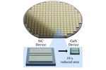
“STMicroelectronics (NYSE:STM), a global semiconductor leader serving customers across the spectrum of electronics applications, and TSMC (TWSE:2330, NYSE: TSM), the world’s largest dedicated semiconductor foundry, are collaborating to accelerate the development of Gallium Nitride (GaN) process technology …

“TSMC has been fast advancing its manufacturing processes. It is on track to move 5nm node to commercial production in the second half of 2020, and will soon break ground for a 3nm facility where volume production will start in …
News TSMC’s N7+ Technology is First EUV Process Delivering Customer Products to Market in High Volume
“TSMC (TWSE: 2330, NYSE: TSM) today announced that its seven-nanometer plus (N7+), the industry’s first commercially available Extreme Ultraviolet (EUV) lithography technology, is delivering customer products to market in high volume. The N7+ process with EUV technology is built …
News TSMC and OIP Ecosystem Partners Deliver Industry’s First Complete Design Infrastructure for 5nm Process Technology
“Enabling next-generation silicon designs targeting advanced mobile and high-performance computing applications TSMC today announced delivery of the complete version of its 5 nanometer (nm) design infrastructure within the Open Innovation Platform® (OIP). This full release enables 5nm systems-on-chip (SoC) designs …