
Other
“In an effort to better study a promising class of materials that could energize the solar cell industry, researchers at Lawrence Berkeley National Laboratory (Berkeley Lab) have developed a new method of analyzing the material’s molecular-scale structure. By combining …
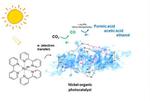
“Scientists have developed a light-activated material that can chemically convert carbon dioxide into carbon monoxide without generating unwanted byproducts. The achievement marks a significant step forward in developing technology that could help generate fuel and other energy-rich products using a …
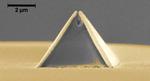
“Combining speed with incredible precision, a team of researchers has developed a way to print a nanoscale imaging probe onto the tip of a glass fiber as thin as a human hair, accelerating the production of the promising new device …
“There’s a known rule-breaker among materials, and a new discovery by an international team of scientists adds more evidence to back up the metal’s nonconformist reputation. According to a new study led by scientists at the Department of …
“Scientists have successfully paired ferroelectric and ferrimagnetic materials so that their alignment can be controlled with a small electric field at near room temperatures, an achievement that could open doors to ultra low-power microprocessors, storage devices and next-generation electronics. The …
News Smallest. Transistor. Ever. - Berkeley Lab-led research breaks major barrier in transistor size by creating gate only 1 nanometer long
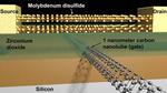
“For more than a decade, engineers have been eyeing the finish line in the race to shrink the size of components in integrated circuits. They knew that the laws of physics had set a 5-nanometer threshold on the size of …
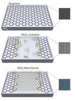
“In an advance that helps pave the way for next-generation electronics and computing technologies—and possibly paper-thin gadgets —scientists with the U.S. Department of Energy’s Lawrence Berkeley National Laboratory (Berkeley Lab) developed a way to chemically assemble transistors …
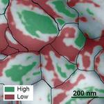
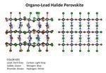
“Scientists from the Department of Energy’s Lawrence Berkeley National Laboratory (Berkeley Lab) have discovered a possible secret to dramatically boosting the efficiency of perovskite solar cells hidden in the nanoscale peaks and valleys of the crystalline material. Solar cells …

“To the growing list of two-dimensional semiconductors, such as graphene, boron nitride, and molybdenum disulfide, whose unique electronic properties make them potential successors to silicon in future devices, you can now add hybrid organic-inorganic perovskites. However, unlike the other contenders …