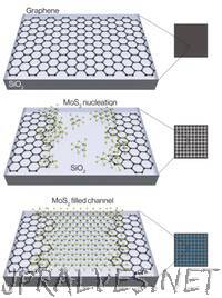
“In an advance that helps pave the way for next-generation electronics and computing technologies—and possibly paper-thin gadgets —scientists with the U.S. Department of Energy’s Lawrence Berkeley National Laboratory (Berkeley Lab) developed a way to chemically assemble transistors and circuits that are only a few atoms thick. What’s more, their method yields functional structures at a scale large enough to begin thinking about real-world applications and commercial scalability.”
Related Content
Related Posts:
- New Map of Space Precisely Measures Nearly 400,000 Nearby Galaxies
- Making Rad Maps With Robot Dogs
- Accelerating Sustainable Semiconductors With ‘Multielement Ink’
- New Consortium to Make Batteries for Electric Vehicles More Sustainable
- Advances in Quantum Emitters Mark Progress Toward a Quantum Internet
- Harnessing Machine Learning to Make Complex Systems More Energy Efficient
- Research on Light Emission From Black Phosphorus Hints at New Applications
- Meet the Autonomous Lab of the Future
- Five Ways QSA is Advancing Quantum Computing
- Electric Vehicle Batteries Could Get Big Boost With New Polymer Coating