
Other
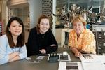
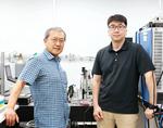
“MIT Professor Frances Ross is pioneering new techniques to study materials growth and how structure relates to performance. A hundred years ago, “2d” meant a two-penny, or 1-inch, nail. Today, “2-D” encompasses a broad range of atomically thin flat materials …
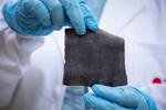
“The next generation of waterproof smart fabrics will be laser printed and made in minutes. That’s the future imagined by the researchers behind new e-textile technology. Scientists from RMIT have developed a cost-efficient and scaleable method for rapidly fabricating …
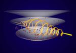
“Research team develops a new principle to generate terahertz radiation The “Landau-level laser” is an exciting concept for an unusual radiation source. It has the potential to efficiently generate so-called terahertz waves, which can be used to penetrate materials as …

“Innovative new electron spectroscopy technique pushes the limits of Nanospectroscopy for materials design In order to understand advanced materials like graphene nanostructures and optimize them for devices in nano-, opto- and quantum-technology it is crucial to understand how phonons – the …
“Atomically thin materials developed by Stanford researchers could create heat-shields for cell phones or laptops that would protect people and temperature-sensitive components and make future electronic gadgets even more compact. Excess heat given off by smartphones, laptops and other electronic …
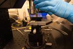
“A technology that can obtain high-resolution, micrometer-sized images for mass spectrometric analysis without sample preparation has been developed. DGIST Research Fellow Jae Young Kim and Chair-professor Dae Won Moon’s team succeeded in developing the precise analysis and micrometer-sized imaging …
“Engineers at the University of California San Diego have developed the thinnest optical device in the world—a waveguide that is three layers of atoms thin. The work is a proof of concept for scaling down optical devices to sizes …
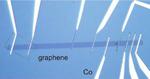
“Researchers from the ICN2 Physics and Engineering of Nanodevices Group have proposed a modified graphene-based nanodevice fabrication technique that has increased up to three times the spin lifetime and relaxation length compared to previous work of the same kind. The …
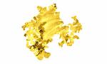
“cientists at the University of Leeds have created a new form of gold which is just two atoms thick – the thinnest unsupported gold ever created. The researchers measured the thickness of the gold to be 0.47 nanometres – one million …
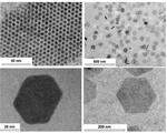
“A KAIST team has designed a novel strategy for synthesizing single-crystalline graphene quantum dots, which emit stable blue light. The research team confirmed that a display made of their synthesized graphene quantum dots successfully emitted blue light with stable electric …