
“Toshiba Electronic Devices & Storage Corporation (“Toshiba”) has developed a new SiC MOSFET device structure that simultaneously achieves higher reliability at high temperatures and lower power loss. In a 3300V chip at 175ºC, a level of current over double that of Toshiba’s present structure, the new structure operates without any loss of reliability, and it also reduces specific on-resistance at room temperature by about 20% for a 3300V chip and 40% for a 1200V chip.
Silicon carbide (SiC) is widely seen as the next generation material for power devices, as it delivers higher voltages and lower losses than silicon. While SiC power devices are now mainly utilized in inverters for trains, wider application is on the horizon, including in photovoltaic power systems and the power management systems of industrial equipment. However, the use and market growth of SiC devices have been held back by reliability issues. One problem is the expansion of crystal defects when current flows through the PN diode [4] positioned between a power MOSFET’s source and drain, which increases on-resistance and degrades device reliability.
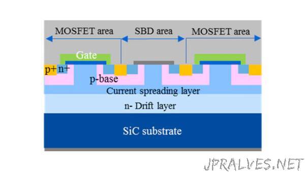
Toshiba developed a novel device structure, a MOSFET with an embedded a schottky barrier diode [5] (SBD) that made progress in solving this problem. This was reported at PCIM Europe 2020, an international power semiconductor conference [6], and introduced into products in August 2020. That structure prevents PN diode operation by positioning an SBD in parallel to the PN diode in the MOSFET; the embedded SBD has a lower on-state voltage than the PN diode, and current flows through it, suppressing changes in on-resistance.
However, that structure can handle only limited current density at high temperatures of 175℃ or more. Accelerated adoption of SiC devices requires SiC devices that maintain high current capability and high reliability at high temperatures.
The new structure is a modification of the SBD-embedded MOSFET device, achieved by applying a 25% process shrink and optimizing the design to strengthen the SBD’s suppression of current in the PN diode. This has realized a 3300V chip structure with more than double the current density at 175℃ compared to Toshiba’s present structure without loss of reliability. The structure also reduces specific on-resistance by about 20% in a 3300V chip and about 40% in a 1200V chip at room temperature.
Details of the achievement were reported at PCIM Europe 2021, and the IEEE-sponsored International Symposium on Power Semiconductor Devices and ICs 2021 (ISPSD 2021), both held online.
Toshiba started sample shipment of a 3.3kV class SiC power module with the new structure in May this year.”