
“As an electrical engineering student, we had a class in the 5th semester that was entirely evaluated on a project done in less than 2.5 months.
This project was a Direct Digital Synthesizer (DDS) based on a Field Programmable Gate Array (FPGA).
After brainstorming the idea was to make a device that synthesizes signals (Sinus, Cosine, Triangle, Saw-tooth, Rectangular and Noise). The frequency range should be between 1Hz and 1MHz, and the whole system should be based on FPGA (Read more about it here and why an FPGA is super cool).
The FPGA was programmed in VHDL- a hardware description language using Xilinx software. The FPGA should have a block memory or a BRAM that has the values of each signal to be synthesized or what is known as a look up table (LUT). The FPGA clock would trigger the LUT that has 1024 values and on each cycle, the value in the respective address will be read and sent as a hexadecimal number (12bit).
The cool thing about FPGA’s everything is done parallel inside its core unlike a microcontroller for example that has to wait a full clock cycle to make a change in a General Purpose Input/Output (GPIO) for example. This allowed the12 bits from the LUT to be sent to 12 different GPIO at the same time.
Since FPGA are only digital interfaces, those 12bits from the different GPIO’s were sent to a 12 bit Digital to analog converter (DAC) which spits out an accurate analog converted signal with the correct clock timing as programmed.
The last step of this system is a two stage operational amplifier (Op-Amp)which converts the differential signal coming out of the DAC to a steady pos/neg signal in the first amplification stage. The second stage of aplification was added to change the amplitude of the output signal.
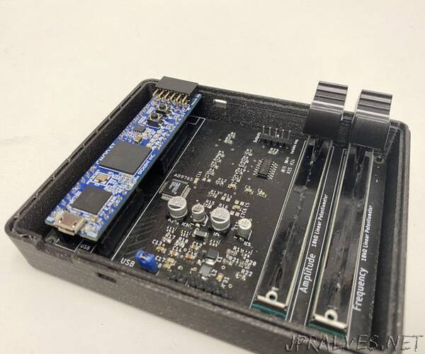
This Instructables will only cover the Printed Circuit Board(PCB) design and schematics. More to the theory of the whole device and how it works follow in the next Instructables.”