
“Retro computer built from 1978-era TTL logic chips. Internet capable with built in web browser and server
Can you browse the Web using pre-1980 TTL logic and memory speeds? The goal of this project is to demonstrate how. Internet connectivity is via an era-appropriate RS232 interface. The machine is upward compatible by a decade to support currently available keyboard and video interfaces (PS/2 and VGA). The video includes a native text mode capable of displaying 96-columns and two bitmapped color graphics modes for retro gaming.
YATAC78 - Yet Another TTL Archaic Computer (1978)
Dual Processor CPU/GPU modified Harvard Architecture.
15.44 MHz machine clock, 7.72 MHz per processor.
256k ROM: 128k program, 96k ALU, 32k fonts.
128K RAM: 78k user data, 50k display.
75 ALU functions including: BCD support, multiply/divide, square root, trigonometry
Bitmapped Graphics 2 resolutions (60Hz refresh): 8 color hi-res mode at 384x256 (4 dithering patterns) or 256 color low-res mode at 192x128 (double buffered).
Text Mode 768x400 native resolution (75Hz refresh). 4 fonts, 96x25 using 8x16 glyphs or 96x50 using 8x8 glyphs. 256 line buffer for 10-page smooth scroll.
8-bit PCM Audio with 4 voices, 20-15kHz bandwidth.
PS2 Keyboard interface built in.
RS232 Serial Port for host/client and network connectivity (up to 115200 baud).
Parallel Port for expansion (4 bits in, 8 bits out, 2 register strobes).
Chip Count 44 TTL, plus single ROM, RAM, PAL, and RS232 driver.
Target PCB size 2 stacked 12cm x 16cm 4-layer boards (24 chips per board).
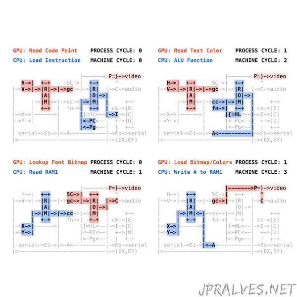
The system is clocked around 15MHz and a typical instruction spans 4 clock cycles as follows:
Load Instruction from ROM.
Read data from source register or RAM.
Perform an ALU function using the ROM as lookup table.
Write data to register, accumulator, and optionally to RAM.
The alternating use of both ROM and RAM allows a second processor to be added to the system. Both processors use dedicated pipelines to cache data between the alternate program and data address spaces. One processor handles serial communications and general computational tasks (CPU) while the other is dedicated to the display and audio (GPU).
The following sequence of diagrams demonstrates the multiplexing of the CPU (shown in blue) and GPU (shown in red). In this example the GPU is operating in text mode and the CPU is executing the sequence described in the numbered list above.
In the first cycle the GPU reads the ASCII code point of a character from the RAM and stores the result in the GPU Cache (gc). The CPU addresses the ROM using the Program Counter (PC) and Page Register (Pg) to load the Instruction Register (I).”