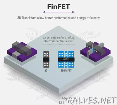
“The ever-increasing demands of today’s electronic devices require smarter, faster semiconductors that use less energy. However, the advancements have been largely based on conventional chip designs, of which their two dimensional configurations are quickly approaching physical limits. The industry’s solution to the dilemma was to adopt three dimensional concepts to semiconductor structures at several different stages of the engineering process, hence ‘3D semiconductor technologies.’ Here are some of the key ‘3D technologies’ that Samsung has introduced to the semiconductor industry, and how they tackled important technical challenges in meeting the market requirements.”
Related Content
Related Posts:
- Samsung Unveils New Portable SSD T5 EVO That Offers 8TB Capacity in a Compact Design
- Samsung Electronics’ Industry-First LPCAMM Ushers in Future of Memory Modules
- Samsung Electronics’ 4TB SSD 990 PRO Series Brings Ultimate Performance and Capacity for Gamers and Creators
- Samsung Electronics Unveils Industry’s Highest-Capacity 12nm-Class 32Gb DDR5 DRAM, Ideal for the AI Era
- Samsung Unveils New PRO Ultimate Memory Cards Designed With Increased Speed and Reliability for Professional Content Creators
- Samsung Develops Industry’s First GDDR7 DRAM To Unlock the Next Generation of Graphics Performance
- Samsung Starts Mass Production of Automotive UFS 3.1 Memory Solution With Industry’s Lowest Power Consumption
- Samsung Electronics and MediaTek Achieve Innovative 5G Uplink Breakthrough With Three Transmit Antennas
- Samsung’s Exynos Auto V920 To Power Hyundai Motor’s Next-Generation In-Vehicle Infotainment Systems
- Samsung Electronics Announces Most Advanced 12nm-Class DDR5 DRAM Has Started Mass Production