Content for S8550

S8550

S8550 is a PNP transistor hence the collector and emitter will be left open (Reverse biased) when the base pin is held at ground and will be closed (Forward biased) when a signal is provided to base pin. It has a maximum gain value of 300; this value determines the amplification capacity of the transistor normally S8550. Since it is very high it is normally used for amplification purposes. When this transistor is fully biased then it can allow a maximum of 700mA to flow across the collector and emitter. This stage is called Saturation Region and the typical voltage allowed across the Collector-Emitter (V­CE) or Collector-Base (VCB) could be 20V and 30V respectively. When base current is removed the transistor becomes fully off, this stage is called as the Cut-off Region.

Giant 555 Timer

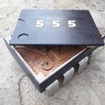
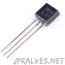
“A Working Replica of the classic 555 timer made using discrete components A fully functional replica of the classic 555 timer made using discrete through hole components which include only basic jellybean components like (to - 92) BJTs , 1/4Watt resistors …