
Other
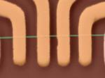
“The new technology has applications in nanometer-scale transistors and circuits Engineers at the University of California, Riverside, have demonstrated prototype devices made of an exotic material that can conduct a current density 50 times greater than conventional copper interconnect technology …
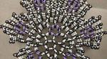
“A new greener, stronger and more durable concrete that is made using the wonder-material graphene could revolutionise the construction industry. Experts from the University of Exeter have developed a pioneering new technique that uses nanoengineering technology to incorporate graphene into …
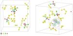
“Perfection is not everything, according to an international team of researchers whose 2-D materials study shows that defects can enhance a material’s physical, electrochemical, magnetic, energy and catalytic properties. “Electronic devices, like transistors, are usually made from relatively bulky …
“Rice scientists show how salt lowers reaction temperatures to make novel materials A dash of salt can simplify the creation of two-dimensional materials, and thanks to Rice University scientists, the reason is becoming clear. Boris Yakobson, a Rice professor of …

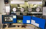
“Commercially available since the 1970s, the lithium-ion battery is now the workhorse power source in many applications. It can be found in cell phones, laptops and electric vehicles. Yet, much about the basic science taking place at the atomic and …
“Newly Conceived Carbon Material Could Become Foundation for Faster, More Efficient Electronics and Quantum Computers The transformative potential of a new carbon material conceived three years ago by two Emirati brothers and an American nuclear scientist may soon be realized …

“A study published in Science reports on how ICFO researchers, with MIT and Univ. of Minho, are able to confine and guide light down to a space of 1-atom thick in dimension. All electronic devices in our daily lives - computers …
“Scalable manufacturing process spools out strips of graphene for use in ultrathin membranes. MIT engineers have developed a continuous manufacturing process that produces long strips of high-quality graphene. The team’s results are the first demonstration of an industrial, scalable …
“A current area of intense interest in nanotechnology is van der Waals heterostructures, which are assemblies of atomically thin two-dimensional (2D) crystalline materials that display attractive conduction properties for use in advanced electronic devices. A representative 2D semiconductor is graphene …
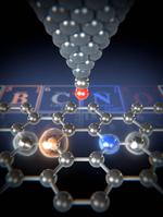
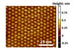
“A team including physicists from the University of Basel has succeeded in using atomic force microscopy to clearly obtain images of individual impurity atoms in graphene ribbons. Thanks to the forces measured in the graphene’s two-dimensional carbon lattice, they …