
“Researchers employ a new “transmetallation” technique to develop ultrathin electronic devices from 2D coordination nanosheets.
Electronically conducting two-dimensional (2D) materials are currently hot topics of research in both physics and chemistry owing to their unique properties that have the potential to open up new avenues in science and technology. Moreover, the combination of different 2D materials, called heterostructures, expands the diversity of their electrical, photochemical, and magnetic properties. This can lead to innovative electronic devices not achievable with a single material alone.
Heterostructures can be fabricated in two ways: vertically, with materials stacked on top of each other, or laterally, where materials are stacked side-by-side on the same plane. Lateral arrangements offer a special advantage, confining charge carriers to a single plane and paving the way for exceptional “in-plane” electronic devices. However, the construction of lateral junctions is challenging.
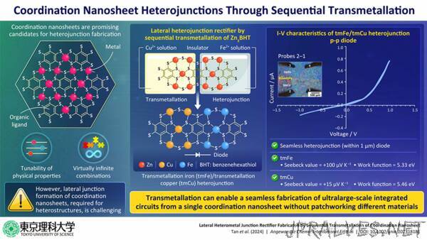
In this regard, conducting 2D materials made using organic materials, called “coordination nanosheets,” are promising. They can be created by combining metals and ligands, ranging from those with metallic properties such as graphene and semiconducting properties such as transition metal dichalcogenides to the ones possessing insulating properties such as boron nitride. These nanosheets enable a unique method called transmetallation. This allows the synthesis of lateral heterostructures with “heterojunctions,” which cannot be achieved through direct reaction. Heterojunctions are interfaces between two materials that have distinct electronic properties and therefore can serve as electronic devices. Furthermore, by utilizing heterojunctions of coordinated nanosheets, new electronic properties that have been difficult to get with conventional 2D materials can be created. Despite these advantages, the research on transmetallation as a method to fabricate heterostructures is still limited.
To address this knowledge gap, a team of researchers from Japan, led by Professor Hiroshi Nishihara from the Research Institute for Science and Technology at Tokyo University of Science (TUS), Japan, used sequential transmetallation to synthesize lateral heterojunctions of Zn3BHT coordination nanosheets. The team included Dr. Choon Meng Tan, Assistant Professor Naoya Fukui, Assistant Professor Kenji Takada, and Assistant Professor Hiroaki Maeda, also from TUS. The study, a joint research effort by TUS, the University of Cambridge, the National Institute for Materials Science (NIMS), Kyoto Institute of Technology, and the Japan Synchrotron Radiation Research Institute (JASRI), was published in the journal Angewandte Chemie International Edition on January 05, 2024.
The team first fabricated and characterized the Zn3BHT coordination nanosheet. Next, they investigated the transmetallation of Zn3BHT with copper and iron. Prof. Nishihara explains: “Via sequential and spatially limited immersion of the nanosheet into aqueous copper and iron ion solutions under mild conditions, we easily fabricated heterostructures with in-plane heterojunctions of transmetallated iron and copper nanosheets.”
This method is a solution process at room temperature and atmospheric pressure, from the fabrication of coordinated nanosheets to the fabrication of in-plane heterojunctions. This process is completely different from the high-temperature, vacuum, gas-phase processing process that is used in lithography technology for silicon semiconductors. It is a simple and inexpensive process that does not require large equipment. The challenge is how to create highly crystalline thin films that are free of impurities. If clean rooms and highly purified reagents are available, commercially viable manufacturing techniques will soon be achieved.
The resulting seamless heterojunction obtained by the researchers demonstrated rectifying behavior common in electronic circuits. Testing the characteristics of the diode revealed the versatility of the Zn3BHT coordination nanosheet. These characteristics can be changed easily without any special equipment. Moreover, this material also enables the fabrication of an integrated circuit from only a single coordination sheet, without any patchworking from different materials. Prof. Nishihara highlights the importance of this technique: “Ultrathin (nanometer-thick) rectifying elements obtained from our method will be quite useful for the fabrication of ultralarge-scale integrated circuits. Simultaneously, the unique physical properties of monoatomic layer films with in-plane heterojunctions can lead to the development of new elements.”
Furthermore, by using this transmetallation reaction, it is possible to create junctions with various electronic properties, such as p-n, MIM (metal-insulator-metal) and MIS (metal-insulator-semiconductor) junctions. The ability to bond single-layer topological insulators will also enable new electronic devices such as electron splitters and multilevel devices that have only been theoretically predicted.
Overall, this study presents a simple yet powerful technique for crafting lateral heterostructures, marking a significant step in 2D materials research.”