
“The speed of innovation in bioelectronics and critical sensors gets a new boost with the unveiling of a technique for fast-prototyping of devices.
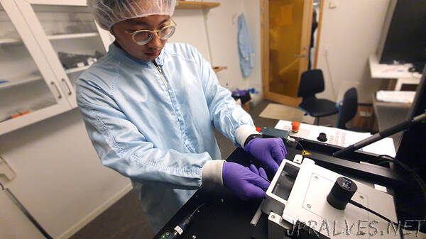
A research team at KTH Royal Institute of Technology and Stockholm University reported a simple way to fabricate electrochemical transistors using a standard Nanoscribe 3D microprinter. Without cleanroom environments, solvents or chemicals, the researchers demonstrated that 3D microprinters can be hacked to laser print and micropattern semiconducting, conducting and insulating polymers.
Anna Herland, professor in Micro- and Nanosystems at KTH, says the printing of these polymers is a key step in prototyping new kinds of electrochemical transistors for medical implants, wearable electronics and biosensors.
The technique could replace time-consuming processes that require an expensive cleanroom environment. Nor would it involve solvents and developer baths that have a negative environmental impact, says the study’s co-author Erica Zeglio, a faculty researcher with Digital Futures, a research center jointly operated by KTH Royal Institute of Technology, Stockholm University and RISE.
“Current methods rely on expensive and unsustainable cleanroom practices,” Zeglio says. “The method we proposed here doesn’t.”
Core component of bioelectronics
Polymers are core components of many bioelectronic and flexible electronic devices. The applications are diverse, including monitoring living tissues and cells and diagnosing diseases in point-of-care testing.
“Fast prototyping of these devices is time consuming and costly.” Herland says. “It hinders the widespread adoption of bioelectronic technologies.”
Using ultrafast laser pulses, the new method creates possibilities for the rapid prototyping and scaling of microscale devices for bioelectronics, says co-author and KTH Professor Frank Niklaus. The team applied the new method to fabricate complementary inverters and enzymatic glucose sensors.
The technique eliminates the need for solvents and lift-off processes such as those used in fabrication of standard electronics. The method could also be used for the patterning of other soft electronic devices, he says.
Herland says the method could advance research in bioelectronic devices and significantly shorten the time-to-market.
“This also creates the possibility of replacing some of the current components with cheaper and more sustainable alternatives,” she says.
The researchers published their results in the journal Advanced Science. Funding was provided in part by Digital Futures, a KTH-based research center that explores and develops digital technologies. Other funders include the Knut and Alice Wallenberg Foundation, Swedish Research Council, European Union’s Horizon 2020 research and innovation program under the Marie Sklodowska-Curie grant agreement, and Formas - a Swedish Research Council for Sustainable Development.
Co-authors also included Alessandro Enrico, Sebastian Buchmann, Fabio De Ferrari, Yunfan Lin, Yazhou Wang, Wan Yue, Gustaf Mårtensson, Göran Stemme and Mahiar Max Hamedi.
Publication
Cleanroom-Free Direct Laser Micropatterning of Polymers for Organic Electrochemical Transistors in Logic Circuits and Glucose Biosensors, Advanced Science, DOI: doi.org/10.1002/advs.202307042”