
“Monash University researchers have demonstrated a new, counterintuitive way to protect atomically-thin electronics — adding vibrations, to reduce vibrations.
By ‘squeezing’ a thin droplet of liquid gallium, graphene devices are painted with a protective coating of glass, gallium-oxide.
This oxide is remarkably thin, less than 100 atoms, yet covers centimetre-wide scales, making it potentially applicable for industrial large-scale fabrication. Current, frontier “2nm” transistors from IBM use gates of similar thickness, close to 10nm (140 atoms).
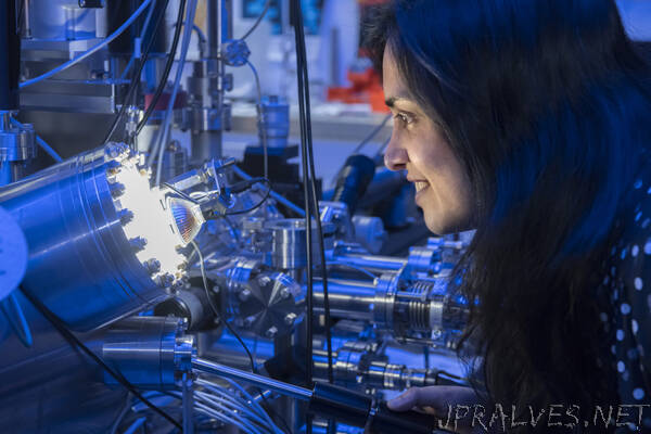
“Mechanically transferring such large-area nanosheets is quite novel,” says lead author Matthew Gebert.
The oxide provides a new method of device protection, whilst also improving device performance:
“The oxide not only enhances and protects our devices when we first transfer it, but also later, during subsequent processing and fabrication,” says co-author Semonti Bhattacharyya.
Gallium-oxide’s enhancing performance is due in part to the material’s high-K dielectric properties, , a key component in the long march towards miniaturising devices and reducing power wastage.
Protective gallium-oxide also yields a surprising result, reducing the electrical resistance in graphene that is caused by thermal vibrations due to heat in the surrounding materials.
“That’s surprising because in effect we are actually adding extra vibrations, to reduce total vibrations,” says Matt.
This is the first time such a strategy to reduce the resistance due to thermal vibrations has been demonstrated in a graphene device.
PROTECTION FROM A DAMAGING ENVIRONMENT
The Monash team from the ARC Centre of Excellence in Future Low-Energy Electronics Technologies (FLEET) used a novel liquid-metal printing technique to create gallium-oxide (Ga2O3) glass. This method was designed by FLEET collaborators at RMIT, who have used the novel glass in a variety of electronics applications.
The glass film that forms on the surface of droplets of liquid gallium metal is more than 5,000 times thinner than a human hair, but can be reliably ‘printed’ from the surface of the liquid metal to form uniform continuous layers over centimetre-sized areas.
The liquid-metal method offers two advantages to protect devices. The layer-printing method prevents growth damage, while the transferred layer is a good barrier for further processing.
Gallium-oxide encapsulation not only offers protection, but can also enhance performance because of its High-K dielectric qualities. High-K dielectrics have not been easy to integrate with graphene, as growth of these materials often involves the bombardment of highly energetic atoms.
As gallium-oxide encapsulation is a mechanical transfer technique (“think forklift stacking,” says Matthew Gebert), it is fundamentally different to alternative deposition methods (such as atomic layer deposition, evaporation, sputtering and vapor deposition) which have undesirable attributes such as high temperature requirements.
Because gallium metal is liquid close to room temperature (30o C), this process has a lot of advantages for industrial adoption. In fact, gallium-oxide can be used as a buffer layer before further processing using these other methods.
The Monash team demonstrated that gallium-oxide protected the graphene from surface damage by testing their graphene devices with industrial growth tools. Depositing another oxide layer damaged only the uncovered areas of graphene, while the areas that were covered by gallium-oxide retained their qualities.
DIELECTRIC LAYERS AND THEIR IMPORTANCE IN COMPUTING
Electrically-insulating (dielectric) materials are particularly important in the function of transistors, the microscopic “switches” at the heart of electronics and computing. These dielectric materials allow a transistor to switch on or off without leaking power, which in turn allows you to use your phone/PC.
To “switch” a transistor, electrons accumulate across the dielectric material to create a voltage and influence the device. However, thinner dielectrics leak current — reducing the ability to switch — and wasting current as heat. High-K dielectrics are important because they increase the effectiveness of the switch, allowing a reduction in current leakage and consequently energy wastage.
However, even high-K dielectrics devices are not impervious to size. As electronic materials get smaller and thinner as we relentlessly march towards cramming-in more transistors (to obey Moore’s Law), materials become strongly influenced by the surfaces of neighbouring materials, often resulting in an drop of performance. This explains why graphene is often damaged by high-K dielectrics.
One of these degrading phenomena that occur at surfaces is material vibrations.
VIBRATIONS AND GALLIUM-OXIDE’S ADVANTAGE
The vibrations of materials due to heat, which cause electrical resistance in materials, are called phonons. These vibrations (phonons) cause the atoms in a solid to oscillate, and flowing electrons bounce off these oscillations and change their direction, leading to electrical resistance.
The thermal vibrations of the carbon atoms in graphene itself cause remarkably little resistance, which is one reason why graphene is such a useful material for electronics.
However, the thin nature of graphene (just one atom thick) means that thermal vibrations in surrounding (remote) materials can have a large effect on electrons in graphene, and these are the predominant cause of electrical resistance in graphene at room temperature.
As temperatures heat up, more phonons are excited, increasing the resistance by scattering electrons.
“You can think of this scenario as a fence,” explains Matt Gebert, who is a PhD candidate at Monash University/FLEET.
“The fence (the 2D graphene) is affected by the actions of neighbours on both sides (the insulating materials on either side of graphene). One neighbour might have a clean environment on their side of the fence (a good insulator, with few phonons) but the other neighbour might have an overgrown garden that damages the fence (a bad insulator with strong phonons) …”
“So in the end, your fence (graphene) doesn’t serve the purpose it was intended to, perhaps not even forming a complete fence (electronic circuit) anymore!”
To investigate the protective qualities of the gallium-oxide, the team mechanically transferred large areas onto graphene devices.
Subsequent measurements confirmed that graphene’s electronic properties at various temperatures and electron populations were maintained — ie, high electron mobility (a very useful property of a transistor) is preserved.
“Surprisingly, adding the layer of Ga2O3 glass reduces the electrical resistance in graphene that is due to phonon scattering,” explains Matt.
(This is true in a target range of temperatures, which is slightly below room temperature.)
“This is counter-intuitive, because by adding this material, you are introducing additional phonons. So you might think: the more phonons, the higher we would expect resistance to be!”
However, these results do agree with existing theories of phonons in insulators. Ga2O3 hosts strong phonons, but this same property also allows it to adjust its own atomic configuration to ‘screen’ the electric field from phonons in the silicon-dioxide glass on the other side of graphene.
Further helping the situation, the strong Ga2O3 phonons are modes that require high energy to populate. As a result, Ga2O3 phonons only becomes active at higher temperatures (with more thermal energy) and this results in lower overall resistance in graphene until a temperature of -53oC (220 K). Gallium-oxide is picking up (only the) good vibrations.
NEW AVENUES TO DEVICE PERFORMANCE.
This strategy, to reduce overall phonons content, is demonstrated for the first time and could be used to identify better-performing hybrid materials at room temperature for 2D electronics.
A similar dielectric material with higher-energy phonon modes than Ga2O3 could partner well with existing silicon technologies, which are currently being pushed to their quantum-scale limits.
The liquid-metal printing technique is a versatile method for industrial partners. The process for touch-printing Ga2O3 scales to large wafer-scale areas, is very automatable and has shown good reproducibility, indicating its merit for industry adoptability.
Gallium metal, which melts at about 30oC, and the transfer equipment are also inexpensive compared to other oxide deposition methods which require large amounts of material or highly elevated temperatures.”