
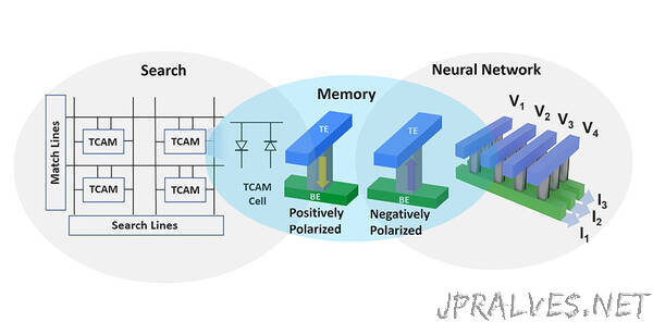
“The transistor-free compute-in-memory architecture permits three computational tasks essential for AI applications: search, storage, and neural network operations.
Artificial intelligence presents a major challenge to conventional computing architecture. In standard models, memory storage and computing take place in different parts of the machine, and data must move from its area of storage to a CPU or GPU for processing.
The problem with this design is that movement takes time. Too much time. You can have the most powerful processing unit on the market, but its performance will be limited as it idles waiting for data, a problem known as the “memory wall” or “bottleneck.”
When computing outperforms memory transfer, latency is unavoidable. These delays become serious problems when dealing with the enormous amounts of data essential for machine learning and AI applications.
As AI software continues to develop in sophistication and the rise of the sensor-heavy Internet of Things produces larger and larger data sets, researchers have zeroed in on hardware redesign to deliver required improvements in speed, agility and energy usage.
A team of researchers from the University of Pennsylvania’s School of Engineering and Applied Science, in partnership with scientists from Sandia National Laboratories and Brookhaven National Laboratory, has introduced a computing architecture ideal for AI.
Co-led by Deep Jariwala, Assistant Professor in the Department of Electrical and Systems Engineering (ESE), Troy Olsson, Associate Professor in ESE, and Xiwen Liu, a Ph.D. candidate in Jarawala’s Device Research and Engineering Laboratory, the research group relied on an approach known as compute-in-memory (CIM).
In CIM architectures, processing and storage occur in the same place, eliminating transfer time as well as minimizing energy consumption. The team’s new CIM design, the subject of a recent study published in Nano Letters, is notable for being completely transistor-free. This design is uniquely attuned to the way that Big Data applications have transformed the nature of computing.
“Even when used in a compute-in-memory architecture, transistors compromise the access time of data,” says Jariwala. “They require a lot of wiring in the overall circuitry of a chip and thus use time, space and energy in excess of what we would want for AI applications. The beauty of our transistor-free design is that it is simple, small and quick and it requires very little energy.”
The advance is not only at the circuit-level design. This new computing architecture builds on the team’s earlier work in materials science focused on a semiconductor known as scandium-alloyed aluminum nitride (AlScN). AlScN allows for ferroelectric switching, the physics of which are faster and more energy efficient than alternative nonvolatile memory elements.
“One of this material’s key attributes is that it can be deposited at temperatures low enough to be compatible with silicon foundries,” says Olsson. “Most ferroelectric materials require much higher temperatures. AlScN’s special properties mean our demonstrated memory devices can go on top of the silicon layer in a vertical hetero-integrated stack. Think about the difference between a multistory parking lot with a hundred-car capacity and a hundred individual parking spaces spread out over a single lot. Which is more efficient in terms of space? The same is the case for information and devices in a highly miniaturized chip like ours. This efficiency is as important for applications that require resource constraints, such as mobile or wearable devices, as it is for applications that are extremely energy intensive, such as data centers.”
In 2021, the team established the viability of the AlScN as a compute-in-memory powerhouse. Its capacity for miniaturization, low cost, resource efficiency, ease of manufacture and commercial feasibility demonstrated serious strides in the eyes of research and industry.
In the most recent study debuting the transistor-free design, the team observed that their CIM ferrodiode may be able to perform up to 100 times faster than a conventional computing architecture.
Other research in the field has successfully used compute-in-memory architectures to improve performance for AI applications. However, these solutions have been limited, unable to overcome the conflicting trade-off between performance and flexibility. Computing architecture using memristor crossbar arrays, a design that mimics the structure of the human brain to support high-level performance in neural network operations, has also demonstrated admirable speeds.
Yet neural network operations, which use layers of algorithms to interpret data and recognize patterns, are only one of several key categories of data tasks necessary for functional AI. The design is not adaptable enough to offer adequate performance on any other AI data operations.
The Penn team’s ferrodiode design offers groundbreaking flexibility that other compute-in-memory architectures do not. It achieves superior accuracy, performing equally well in not one but three essential data operations that form the foundation of effective AI applications. It supports on-chip storage, or the capacity to hold the enormous amounts of data required for deep learning, parallel search, a function that allows for accurate data filtering and analysis, and matrix multiplication acceleration, the core process of neural network computing.
“Let’s say,” says Jariwala, “that you have an AI application that requires a large memory for storage as well as the capability to do pattern recognition and search. Think self-driving cars or autonomous robots, which need to respond quickly and accurately to dynamic, unpredictable environments. Using conventional architectures, you would need a different area of the chip for each function and you would quickly burn through the availability and space. Our ferrodiode design allows you to do it all in one place by simply changing the way you apply voltages to program it.”
The payoff of a CIM chip that can adapt to multiple data operations is clear: When the team ran a simulation of a machine learning task through their chip, it performed with a comparable degree of accuracy to AI-based software running on a conventional CPU.
“This research is highly significant because it proves that we can rely on memory technology to develop chips that integrate multiple AI data applications in a way that truly challenges conventional computing technologies,” says Liu, the first author on the study.
The team’s design approach is one that takes into account that AI is neither hardware nor software, but an essential collaboration between the two.
“It is important to realize that all of the AI computing that is currently done is software-enabled on a silicon hardware architecture designed decades ago,” says Jariwala. “This is why artificial intelligence as a field has been dominated by computer and software engineers. Fundamentally redesigning hardware for AI is going to be the next big game changer in semiconductors and microelectronics. The direction we are going in now is that of hardware and software co-design.”
“We design hardware that makes software work better,” adds Liu, “and with this new architecture we make sure that the technology is not only fast, but also accurate.”
John Ting, Yunfei He, Merrilyn Mercy Adzo Fiagbenu, Jeffrey Zheng, Dixiong Wang, Jonathan Frost, Pariasadat Musavigharavi, Surendra B. Anantharaman of the University of Pennsylvania contributed to this research. Eric A. Stach, Robert D. Bent Professor of Engineering in the Department of Materials Science and Engineering and Director of the Laboratory for Research on the Structure of Matter at the University of Pennsylvania also contributed. Further contributions were provided by Giovanni Esteves of Sandia National Laboratories and Kim Kisslinger of Brookhaven National Laboratory.
This work was supported by the Defense Advanced Research Projects Agency (DARPA), Tunable Ferroelectric Nitrides (TUFEN) Program under Grant HR 00112090047. The work was carried out in part at the Singh Center for Nanotechnology at the University of Pennsylvania which is supported by the National Science Foundation (NSF) National Nanotechnology Coordinated Infrastructure Program (NSF Grant NNCI 1542153). Use of facilities and instrumentation supported by NSF through the University of Pennsylvania Materials Research Science and Engineering Center (MRSEC) (DMR-1720530). Support from the Intel RSA program is acknowledged. This research used resources of the Center for Functional Nanomaterials, which is a US Department of Energy Office of Science User Facility, at Brookhaven National Laboratory under Contract No. DE SC0012704. Sandia National Laboratories is a multimission laboratory managed and operated by National Technology & Engineering Solutions of Sandia, LLC, a wholly owned subsidiary of Honeywell International Inc., for the U.S. Department of Energy’s National Nuclear Security Administration under contract DE NA000352.”