
“Rice University models show unique properties of 2D materials stressed by contoured substrates
Atoms do weird things when forced out of their comfort zones. Rice University engineers have thought up a new way to give them a nudge.
Materials theorist Boris Yakobson and his team at Rice’s George R. Brown School of Engineering have a theory that changing the contour of a layer of 2D material, thus changing the relationships between its atoms, might be simpler to do than previously thought.
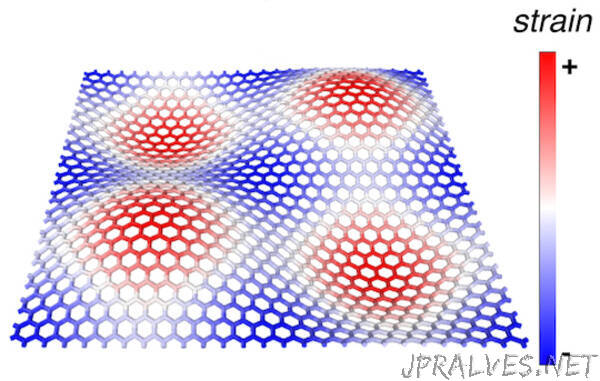
While others twist 2D bilayers — two layers stacked together — of graphene and the like to change their topology, the Rice researchers suggest through computational models that growing or stamping single-layer 2D materials on a carefully designed undulating surface would achieve “an unprecedented level of control” over their magnetic and electronic properties.
They say the discovery opens a path to explore many-body effects, the interactions between multiple microscopic particles, including quantum systems.
The paper by Yakobson and two alumni, co-lead author Sunny Gupta and Henry Yu, of his lab appears in Nature Communications.
The researchers were inspired by recent discoveries that twisting or otherwise deforming 2D materials bilayers like bilayer graphene into “magic angles” induced interesting electronic and magnetic phenomena, including superconductivity.
Their models show that rather than twisting, simply stamping or growing a 2D material like hexagonal boron nitride (hBN) onto a bumpy surface naturally strains the material’s lattice, allowing it to form pseudo-electric and pseudo-magnetic fields and possibly exhibit rich physical effects similar to those found in twisted materials.
Flat hBN is an insulator, but the researchers found that straining the atoms in their model created band structures, effectively making it a semiconductor.
The advantage to their strategy, Gupta said, is that the deformation would be highly controllable through the surface bumps, as substrates could be accurately patterned using electron-beam lithography. “This will also allow one to controllably change the electronic states and quantum effects by designing substrates with different topography,” he said.
Because the charge can be manipulated to flow in one direction, the path it follows is a model for 1D systems. Yakobson said that can be used to explore properties of 1D quantum systems that can’t be accessed through twisted graphene.
“Imagine a road with a single lane such that the cars are allowed to move in only one direction,” Gupta said. “A car cannot overtake the one in front, so traffic will move only when all cars move collectively.
“This is not the case in 2D or when you have multiple lanes, where the cars — or electrons — can pass,” he said. “Like cars, electrons in a 1D system will flow collectively and not individually. This makes 1D systems special with rich, unexplored physics.”
Gupta said it would be much easier to form a bumpy substrate with an electron beam than it currently is to twist 2D bilayers of graphene or other heterostructures like hBN to less than a single degree of accuracy.
“Moreover, one can realize 1D quantum states, which are not typically accessible by twisting 2D bilayers,” he said. “This will allow for the exploration of physical effects in 1D that have remained largely elusive until now.”
Yakobson is the Karl F. Hasselmann Professor of Engineering and a professor of materials science and nanoengineering and of chemistry.
The U.S. Army Research Office (W911NF-16-1-0255) and the Office of Naval Research (N00014-18-1-2182) supported the research. Computing resources were provided by the National Science Foundation XSEDE facility.”