
“Design Also Poised To Save Space, Retain Memory In Event Of Power Loss
A new spin on one of the 20th century’s smallest but grandest inventions, the transistor, could help feed the world’s ever-growing appetite for digital memory while slicing up to 5% of the energy from its power-hungry diet.
Following years of innovations from the University of Nebraska–Lincoln’s Christian Binek and University at Buffalo’s Jonathan Bird and Keke He, the physicists recently teamed up to craft the first magneto-electric transistor.
Along with curbing the energy consumption of any microelectronics that incorporate it, the team’s design could reduce the number of transistors needed to store certain data by as much as 75%, said Nebraska physicist Peter Dowben, leading to smaller devices. It could also lend those microelectronics steel-trap memory that remembers exactly where its users leave off, even after being shut down or abruptly losing power.
“The implications of this most recent demonstration are profound,” said Dowben, who co-authored a recent paper on the work that graced the cover of the journal Advanced Materials.
Many millions of transistors line the surface of every modern integrated circuit, or microchip, which itself is manufactured in staggering numbers — roughly 1 trillion in 2020 alone — from the industry-favorite semiconducting material, silicon. By regulating the flow of electric current within a microchip, the tiny transistor effectively acts as a nanoscopic on-off switch that’s essential to writing, reading and storing data as the 1s and 0s of digital technology.
But silicon-based microchips are nearing their practical limits, Dowben said. Those limits have the semiconductor industry investigating and funding every promising alternative it can.
“The traditional integrated circuit is facing some serious problems,” said Dowben, Charles Bessey Professor of physics and astronomy at Nebraska. “There is a limit to how much smaller it can get. We’re basically down to the range where we’re talking about 25 or fewer silicon atoms wide. And you generate heat with every device on an (integrated circuit), so you can’t any longer carry away enough heat to make everything work, either.”
That predicament looms even as the demand for digital memory, and the energy needed to accommodate it, have soared amid the widespread adoption of computers, servers and the internet. The microchip-enabled smartening of TVs, vehicles and other technology has only increased that demand.
“We’re getting to the point where we’re going to approach the previous energy consumption of the United States just for memory (alone),” Dowben said. “And it doesn’t stop.
“So you need something that you can shrink smaller, if possible. But above all, you need something that works differently than a silicon transistor, so that you can drop the power consumption, a lot.”
‘Now that it works, the fun begins’
Typical silicon-based transistors consist of multiple terminals. Two of them, called the source and drain, serve as the starting and end points for electrons flowing through a circuit. Above that channel sits another terminal, the gate. Applying voltage between the gate and source can dictate whether the electric current flows with low or high resistance, leading to either a buildup or absence of electron charges that gets encoded as a 1 or 0, respectively. But random-access memory — the form that most computer applications rely on — requires a constant supply of power just to maintain those binary states.
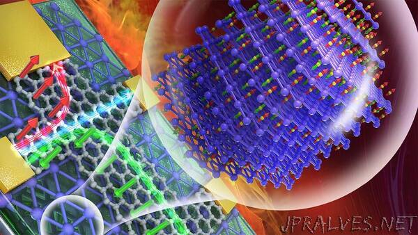
So rather than depend on electric charge as the basis of its approach, the team turned to spin: a magnetism-related property of electrons that points up or down and can be read, like electric charge can, as a 1 or 0. The team knew that electrons flowing through graphene, an ultra-robust material just one atom thick, can maintain their initial spin orientations for relatively long distances — an appealing property for demonstrating the potential of a spintronic-based transistor. Actually controlling the orientation of those spins, using substantially less power than a conventional transistor, was a much more challenging prospect.
To do it, the researchers needed to underlay the graphene with the right material. Fortunately, Binek had already dedicated years to studying and modifying just such a material, chromium oxide. Crucially, chromium oxide is magneto-electric, meaning that the spins of the atoms at its surface can be flipped from up to down, or vice versa, by applying a meager amount of temporary, energy-sipping voltage.
When applying positive voltage, the spins of the underlying chromium oxide point up, ultimately forcing the spin orientation of the graphene’s electric current to veer left and yield a detectable signal in the process. Negative voltage instead flips the spins of the chromium oxide down, with the spin orientation of the graphene’s current flipping to the right and generating a signal clearly distinguishable from the other.
“Now you are starting to get really good fidelity (in the signal), because if you’re sitting on one side of the device, and you’ve applied a voltage, then the current is going this way. You can say that’s ‘on,’” Dowben said. “But if it’s telling the current to go the other way, that’s clearly ‘off.’
“This potentially gives you huge fidelity at very little energy cost. All you did was apply voltage, and it flipped.”
As promising and functional as the team’s demonstration was, Dowben said there exist plenty of alternatives to graphene that share its one-atom thickness but also boast properties better suited to a magneto-electric transistor. The race to overlay chromium oxide with those other 2D candidates is already on, he said, and marks “not the something, but the start of something.”
“Now that it works, the fun begins, because everybody’s going to have their own favorite 2D material, and they’re going to try it out,” Dowben said. “Some of them will work a lot, lot better, and some won’t. But now that you know it works, it’s worth investing in those other, more sophisticated materials that could.
“Now everybody can get into the game, figuring out how to make the transistor really good and competitive and, indeed, exceed silicon.”
Arriving at that point was a long journey paved with “a humongous number of advances,” Dowben said, particularly from the duo of Binek and Bird.
“This kind of project demonstrates how impactful and effective collaborative research can be,” Bird said, “combining, as it does, the renowned expertise in magnetic materials at Nebraska with Buffalo’s capabilities in nanoscale semiconductor devices.”
Dowben recounted just a few of the team’s essential advances. There was the realization that magneto-electric materials could prove a workable approach. The identification of chromium oxide. The modification of it, both to control its spin with voltage instead of power-draining magnetism, but also to ensure it would operate well above room temperature — because, as Dowben put it, “If you’re going to compete with the semiconductor industry, it can’t just work in Nebraska in the winter. It has to work in Saudi Arabia in the summer.” Then there were the theory-backed computer simulations and multiple early-stage prototypes.
“There was no Edisonian moment here. You kind of know where you’re going, but it takes a while,” Dowben said. “There are a lot of technical problems to solve. It’s a slog, and it don’t look pretty.
“But sometimes the outcomes are absolutely spectacular,” he said, “and it’s fun.”
The team received support from the National Science Foundation’s Established Program to Stimulate Competitive Research, which funded the $20 million Emergent Quantum Materials and Technologies collaboration at Nebraska, and from the Semiconductor Research Corporation.”